 ChipApex | Global Electronic Components Supplier
SEARCH
Search Product
Search Post
— IC芯片 | 连接器 | 传感器 | 被动器件 —
Search productSearch post
— IC芯片 | 连接器 | 传感器 | 被动器件 —
Consult the customer manager about the wholesale price.
consultation hotline:86-132-6715-2157
email:[email protected]
Contact the product manager for consultation. One-stop consultation is available.
Do you want a lower wholesale price? Please send us your inquiry and we will reply immediately.
The MC88916EG80 is a low skew CMOS PLL clock driver with processor reset functionality, manufactured by Renesas Electronics Corporation. It utilizes phase-locked loop technology to lock output frequency and phase onto an input reference clock, designed for CISC microprocessor or single processor RISC systems. The device operates within a supply voltage range of 4.5V to 5.5V and supports frequencies up to 80MHz on the 2X_Q output. It features six outputs (Q0–Q2, Q3, 2X_Q, Q/2) with minimal skew, TTL-level compatible inputs, and CMOS/TTL level outputs. Packaged in a 20-SOIC surface mount case, it includes specific reset control pins for the MC68/EC/LC030/040 microprocessor family.
Verify the manufacturer designation, as the component history involves transitions from Motorola to Freescale Semiconductor and subsequently to Integrated Device Technology (IDT), which was acquired by Renesas. Ensure the specific suffix matches the required speed grade (70MHz or 80MHz) and package type (DW suffix for SOIC). Confirm RoHS compliance status based on the specific production lot and revision, as older datasheets may reflect pre-compliance manufacturing standards.
Select the MC88916DW80 variant if the system requires a maximum 2X_Q output frequency of 80MHz (40MHz Q outputs). Choose the MC88916DW70 variant for systems operating up to 70MHz 2X_Q (35MHz Q outputs). Ensure the application provides a separate analog power supply isolation scheme using the recommended loop filter components (RC1 pin circuitry) to minimize jitter. Verify that the SYNC input frequency falls within the specified range of 5MHz to FMax/4.
The MC88916 belongs to the IDT Low Skew CMOS PLL Clock Driver series, originally developed by Motorola Timing Solutions. The product line was transferred to Freescale Semiconductor's Timing Solutions Organization before being acquired by Integrated Device Technology, Inc. Renesas Electronics Corporation now holds the rights to this legacy timing solution portfolio. This component serves as a specialized interface between system clocks and high-performance processors like the 68040.
Public confirmed substitute part numbers are not available in the provided documentation. Designers targeting 68040 PCLK and BCLK inputs at lower frequencies should refer to the MC88920 data sheet, as the MC88916 2X_Q output does not meet the stringent duty cycle requirements for those specific low-frequency inputs.
If RST_IN is held high during power-up, RST_OUT remains low until the PLL achieves steady-state phase/frequency lock to the input reference. After lock is achieved, RST_OUT goes high impedance after 1024 'Q' output cycles, allowing an external pull-up resistor to raise the signal.
The 1MΩ resistor injects current into the internal charge pump of the PLL to prevent excessive jitter caused by inherent PLL dead-band. It also creates a fixed phase offset between the SYNC input and the Q0 output, which must be accounted for in timing calculations.
No, the 2X_Q output does not meet the stringent duty cycle requirement for the 20MHz and 25MHz 68040 microprocessor PCLK input. For these lower frequencies, the MC88920 is the designated component.
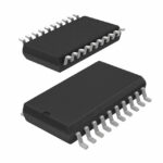 MC88916EG80
The activity of extra discounts on wholesale prices is in full swing…
Please fill in your contact information and we will send you the latest wholesale price list.





