ChipApex | Global Electronic Components Supplier

SEARCH
Search Product
Search Post
— IC芯片 | 连接器 | 传感器 | 被动器件 —
Search productSearch post
— IC芯片 | 连接器 | 传感器 | 被动器件 —
Consult the customer manager about the wholesale price.
consultation hotline:86-132-6715-2157
email:[email protected]
Contact the product manager for consultation. One-stop consultation is available.
Do you want a lower wholesale price? Please send us your inquiry and we will reply immediately.
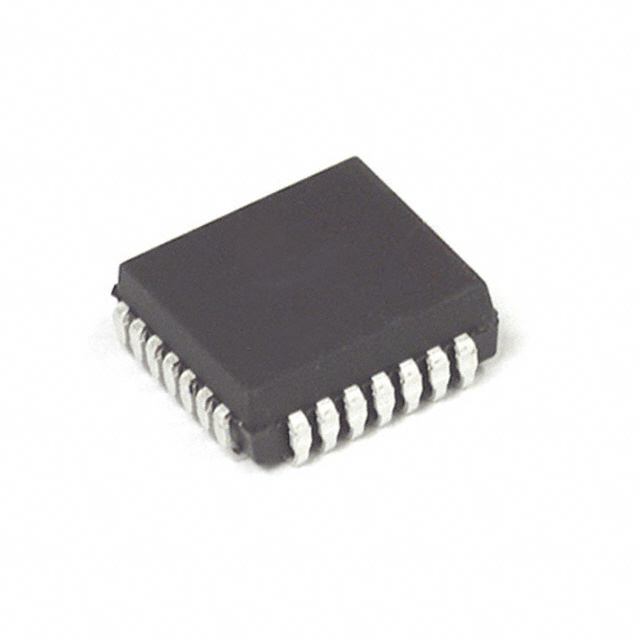
MC88LV915TFN is listed in the Clock Generators, PLLs, Frequency Synthesizers range at ChipApex. The manufacturer field lists NXP USA Inc.. Its product description is IC CLOCK DRIVER 28PLCC. Review the specifications below when checking this part for your BOM.
The MC88LV915TFN is a low skew CMOS PLL clock driver designed for high-performance PC and workstation clock distribution. It locks multiple outputs to an input reference clock with minimal delay. The device provides five Q outputs (Q0–Q4) with less than 500 ps skew, an inverted Q5 output, a 2X_Q output running at twice the frequency, and a Q/2 output. It operates on a single 3.3V supply within a 0°C to 70°C temperature range. Maximum operating frequencies are 100 MHz for the 2X_Q output and 50 MHz for the Q outputs. Outputs feature ±36 mA drive capability compatible with CMOS and TTL levels.
Verify the FN suffix indicates a Plastic PLCC package (Case 776-02). Confirm the device meets the recommended operating conditions of 3.3V ±0.3V supply voltage and 0°C to 70°C ambient temperature. Ensure loop filter components match the datasheet recommendations for stable operation.
Select this component when low skew distribution from a single reference is required. The FREQ_SEL pin allows divide-by-2 feedback for optimal VCO operation with low-frequency inputs. Use the OE/RST pin for 3-state control during board testing. Ensure the input frequency falls between 5 MHz and the respective Fmax specification.
Originally manufactured by Motorola, Inc., this part is now distributed under NXP USA Inc. branding following corporate acquisitions. The datasheet revision is Rev 3, dated 08/2001. The device belongs to the MC88LV series of low voltage clock drivers.
Public confirmed substitute part numbers are not available in the provided documentation. Verify compatibility with existing loop filter designs if substituting with other PLL clock drivers.
The FREQ_SEL pin selects between divide-by-1 and divide-by-2 in the PLL feedback path. Holding it low (÷2) allows the VCO to run in its optimal range (>20MHz) when using a low-frequency reference clock.
Holding PLL_EN high enables normal phase-locked operation. Pulling it low disables the VCO and puts the device in a static test mode, allowing the input clock to bypass the VCO for low-frequency board testing.
The LOCK output goes high when the loop achieves steady-state phase and frequency lock. It goes low if phase-lock is lost or if the PLL_EN pin is low. It asserts no later than 10ms after receiving a SYNC signal and full power.
Explore related parts through Clock/Timing, Integrated Circuits (ICs), all product categories, ChipApex homepage.
 MC88LV915TFN

The activity of extra discounts on wholesale prices is in full swing…
Please fill in your contact information and we will send you the latest wholesale price list.