 ChipApex | Global Electronic Components Supplier

SEARCH
Search Product
Search Post
— IC芯片 | 连接器 | 传感器 | 被动器件 —
Search productSearch post
— IC芯片 | 连接器 | 传感器 | 被动器件 —
Consult the customer manager about the wholesale price.
consultation hotline:86-132-6715-2157
email:[email protected]
Contact the product manager for consultation. One-stop consultation is available.
Do you want a lower wholesale price? Please send us your inquiry and we will reply immediately.
MCP3901T-I/SS is listed in the Analog Front End (AFE) range at ChipApex. The manufacturer field lists Microchip Technology. Its product description is IC AFE 2 CHAN 24BIT 20SSOP. Review the specifications below when checking this part for your BOM.
The MCP3901T-I/SS is a dual-channel Analog Front End (AFE) featuring two synchronous sampling 16/24-bit Delta-Sigma ADCs. It operates with independent analog (AVDD: 4.5V-5.5V) and digital (DVDD: 2.7V-5.5V) supplies. Key electrical specifications include 91 dB SINAD, -104 dBc THD, and 109 dB SFDR per channel. The device supports programmable data rates up to 64 ksps, internal voltage reference drift of 12 ppm/°C, and crosstalk of -133 dB. It includes high-gain PGAs (up to 32 V/V), phase delay compensation, and a 20 MHz SPI interface. Typical power consumption is 14 mW at 5V.
Verify the 'I' suffix indicates the Industrial temperature range (-40°C to +85°C). Confirm the 'T' suffix corresponds to tape-and-reel packaging if reel quantity is required. Ensure AVDD and DVDD supply voltages match the specified ranges for proper operation. Check pinout compatibility for the 20-lead SSOP package.
Select this component when synchronous sampling of two channels is required for accurate power calculations. Ensure the master clock frequency falls within the 1-5 MHz range (or up to 8.192 MHz with boost) for specified accuracy. Verify that the input signal amplitude fits within the PGA gain-adjusted linear range of ±500 mV/GAIN relative to the 2.4V reference.
The MCP3901T-I/SS belongs to the MCP3901 family of dual-channel AFEs. The 'T' denotes tape-and-reel packaging, while 'I' specifies the industrial temperature grade. The '/SS' indicates the 20-lead Small Shrink Outline Package (SSOP). This part integrates ADCs, PGAs, and a voltage reference into a single compact solution.
Check Microchip's official cross-reference documentation for verified substitutes. Ensure any replacement maintains dual-channel synchronous sampling capability and compatible SPI interface timing. Verify thermal resistance and package dimensions if board space is constrained.
The analog input pins can withstand an absolute voltage of ±6V with respect to AGND continuously without damage. However, the specified linear operating range is limited to ±1V with no distortion.
By default, the DR_HIZN bit is set to 0, making the DR pin high-impedance. It should be pulled up to DVDD via a 100 kΩ resistor if used as an interrupt source.
Yes, by setting the CLKEXT bit to 1, the internal crystal oscillator is disabled. An external clock source can then be applied directly to the OSC1/CLKI pin.
Explore related parts through Data Acquisition, Integrated Circuits (ICs), all product categories, ChipApex homepage.
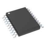 MCP3901T-I/SS

The activity of extra discounts on wholesale prices is in full swing…
Please fill in your contact information and we will send you the latest wholesale price list.





