 ChipApex | Global Electronic Components Supplier
SEARCH
Search Product
Search Post
— IC芯片 | 连接器 | 传感器 | 被动器件 —
Search productSearch post
— IC芯片 | 连接器 | 传感器 | 被动器件 —
Consult the customer manager about the wholesale price.
consultation hotline:86-132-6715-2157
email:[email protected]
Contact the product manager for consultation. One-stop consultation is available.
Do you want a lower wholesale price? Please send us your inquiry and we will reply immediately.
The MCP4812T-E/MS is a dual-channel, 10-bit buffered voltage output Digital-to-Analog Converter (DAC) manufactured by Microchip Technology. It features an SPI-compatible serial interface supporting up to 20 MHz clock speeds and includes a 2.048V internal voltage reference with a 50 ppm/°C temperature coefficient. The device operates on a single supply voltage ranging from 2.7V to 5.5V and offers selectable unity or 2x gain outputs. Key electrical specifications include a typical settling time of 4.5 µs, rail-to-rail output capability, and an operating temperature range from -40°C to +125°C. It is housed in an 8-lead MSOP package.
Verify the 'T' suffix indicates tape-and-reel packaging when ordering. Confirm the '-E' designation corresponds to the extended industrial temperature range (-40°C to +125°C). Ensure the '/MS' suffix matches the required MSOP-8 surface-mount package. Cross-reference the specific datasheet revision to confirm pinout and timing parameters remain consistent with current design requirements.
Select this component for applications requiring dual-channel DAC functionality with moderate resolution and fast settling times. The internal reference eliminates the need for external precision references, simplifying board layout. Consider the 2x gain option if higher output voltage swing is necessary within the supply limits. Verify that the load capacitance does not exceed specifications to maintain stability without oscillation.
This part belongs to the MCP48xx series of dual-channel DACs, which also includes the 8-bit MCP4802 and 12-bit MCP4822 variants. These devices share identical pinouts, interfaces, and general electrical characteristics, differing primarily in resolution and associated linearity errors. The series is designed for cost-sensitive consumer and industrial applications requiring reliable digital-to-analog conversion.
The MCP4812-E/MS is the tube-packaged equivalent of the MCP4812T-E/MS. Other family members like the MCP4802 or MCP4822 offer different resolutions but maintain pin compatibility. External alternatives may require level shifting or additional components to match the integrated reference and gain capabilities.
The output range is set by the internal 2.048V reference and a configurable gain bit. With 1x gain, the range is 0 to 2.048V; with 2x gain, it is 0 to 4.096V.
In shutdown mode, internal circuits are powered down to save energy, and the output amplifier presents a high impedance (typically 500 kΩ) to the load.
Yes, the LDAC pin allows synchronous updating of both DAC registers, ensuring both outputs change at the same time.
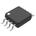 MCP4812T-E/MS
The activity of extra discounts on wholesale prices is in full swing…
Please fill in your contact information and we will send you the latest wholesale price list.






