 ChipApex | Global Electronic Components Supplier
SEARCH
Search Product
Search Post
— IC芯片 | 连接器 | 传感器 | 被动器件 —
Search productSearch post
— IC芯片 | 连接器 | 传感器 | 被动器件 —
Consult the customer manager about the wholesale price.
consultation hotline:86-132-6715-2157
email:[email protected]
Contact the product manager for consultation. One-stop consultation is available.
Do you want a lower wholesale price? Please send us your inquiry and we will reply immediately.
The MCP4821T-E/MC is a single-channel, 12-bit buffered voltage output Digital-to-Analog Converter (DAC) manufactured by Microchip Technology. It operates on a single supply voltage ranging from 2.7V to 5.5V and features an internal 2.048V voltage reference. The device utilizes a resistive string architecture with SPI compatibility supporting up to 20 MHz clock speeds. Key electrical parameters include a typical settling time of 4.5 µs, operating current of 330 µA at 5V, and rail-to-rail output swing. It supports selectable unity or 2x gain outputs and includes hardware shutdown capabilities.
Verify the specific suffix 'MC' against official datasheets to confirm package type and tape/reel specifications. Ensure the ordering code matches the required temperature range and packaging format. Cross-reference the manufacturer part number with distributor listings to confirm availability and authenticity before procurement.
Select this component when a single-channel, 12-bit resolution is required with integrated reference capabilities. Consider the 2.7V to 5.5V supply range and SPI interface compatibility with the host microcontroller. Evaluate the 4.5 µs settling time and low power consumption against system performance requirements.
This device belongs to the MCP4801/4811/4821 family of voltage output DACs. It shares architectural similarities with the MCP4801 (8-bit) and MCP4811 (10-bit), differing primarily in resolution. Related products include dual-channel variants like the MCP4822 and external reference versions such as the MCP4921.
Direct substitutes within the same family include MCP4821T-E/SN and MCP4821-E/MS. Verify pinout compatibility and thermal resistance differences between MSOP, SOIC, and DFN packages when replacing.
The SHDN pin allows hardware control of the shutdown mode. When driven low, it turns off most internal circuits to save power, configuring the output to a known high-resistance state.
The full-scale range is configured by setting the Gain Selection bit in the configuration register. A gain of 1x results in a 2.048V range, while a gain of 2x results in a 4.096V range.
The LDAC pin transfers data from the input latch register to the DAC register, enabling synchronized updates of the analog output voltage across multiple devices if used in conjunction with other DACs.
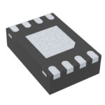 MCP4821T-E/MC
The activity of extra discounts on wholesale prices is in full swing…
Please fill in your contact information and we will send you the latest wholesale price list.





