 ChipApex | Global Electronic Components Supplier
SEARCH
Search Product
Search Post
— IC芯片 | 连接器 | 传感器 | 被动器件 —
Search productSearch post
— IC芯片 | 连接器 | 传感器 | 被动器件 —
Consult the customer manager about the wholesale price.
consultation hotline:86-132-6715-2157
email:[email protected]
Contact the product manager for consultation. One-stop consultation is available.
Do you want a lower wholesale price? Please send us your inquiry and we will reply immediately.
The MCP48CMB14-E/ML is a quad-channel, 10-bit buffered voltage output Digital-to-Analog Converter (DAC) manufactured by Microchip Technology. It features Multi-Time Programmable (MTP) nonvolatile memory for power-up output values and configuration registers. The device operates on a single supply voltage ranging from 2.7V to 5.5V, with reduced specifications available between 1.8V and 2.7V. It utilizes an SPI serial interface supporting write speeds up to 50 MHz and read speeds up to 25 MHz. The component provides selectable gain options of 1x or 2x and supports multiple voltage reference sources including VDD, external VREF, or an internal band gap. It is housed in a 20-lead QFN package.
Verify the specific ordering suffix against official Microchip documentation to confirm package type and temperature range. Ensure compatibility with system voltage levels, particularly regarding the 1.8V to 2.7V reduced specification range if operating below 2.7V. Confirm that the high-voltage programming requirements for the MTP memory are supported by the host controller circuitry before finalizing procurement.
Select this component when quad-channel 10-bit resolution with nonvolatile retention is required. Compare against volatile variants like the MCP48CVB14 if power loss persistence is unnecessary. Consider the MCP48CMB04 or MCP48CMB24 if different resolutions are preferred. Verify that the 20-lead QFN package fits the PCB layout constraints and thermal requirements of the design.
This part belongs to the MCP48CXBX4/8 family of digital-to-analog converters. It shares architectural similarities with other members of the series, differing primarily in channel count, resolution, and memory type. The 'C' indicates commercial temperature range, 'M' denotes MTP memory, 'B' signifies buffered output, '1' represents 10-bit resolution, and '4' indicates four channels.
Public confirmed substitute part numbers: MCP48CMB14T-E/ML (tape and reel packaging variant).
The MTP memory can be written by the user up to 32 times for each specific register location. After 32 cycles, subsequent writes are inhibited.
The LAT/HVC pin serves a dual purpose. It acts as a latch input for simultaneous updating of DAC outputs and requires a high-voltage level (typically 7.5V) to program the MTP memory locations.
Yes, the device supports operation down to 1.8V, but analog specifications are reduced in this range compared to the full 2.7V to 5.5V operating range.
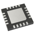 MCP48CMB14-E/ML
The activity of extra discounts on wholesale prices is in full swing…
Please fill in your contact information and we will send you the latest wholesale price list.






