 ChipApex | Global Electronic Components Supplier
SEARCH
Search Product
Search Post
— IC芯片 | 连接器 | 传感器 | 被动器件 —
Search productSearch post
— IC芯片 | 连接器 | 传感器 | 被动器件 —
Consult the customer manager about the wholesale price.
consultation hotline:86-132-6715-2157
email:[email protected]
Contact the product manager for consultation. One-stop consultation is available.
Do you want a lower wholesale price? Please send us your inquiry and we will reply immediately.
The MCP6S92-E/MS is a dual-channel, single-supply analog Programmable Gain Amplifier (PGA) from Microchip Technology. It features an integrated input multiplexer selectable via a Serial Peripheral Interface (SPI). The device supports gains ranging from +1 V/V to +32 V/V with low gain error and rail-to-rail input/output capabilities. Key electrical specifications include a maximum input offset voltage of 4 mV, typical quiescent current of 1.0 mA, and operation within a supply voltage range of 2.5V to 5.5V. It is housed in an 8-lead MSOP package and rated for extended industrial temperatures from -40°C to +125°C.
Verify the specific suffix 'E' indicates the extended temperature grade (-40°C to +125°C) and 'MS' denotes the 8-lead MSOP package. Confirm that the datasheet DS21908A applies to this variant. Ensure the design accounts for the internal connection of the VREF pin to VSS on the MCP6S92 model, which differs from other family members.
Select this component when a dual-input programmable gain amplifier is required for single-supply systems. The MCP6S92 is suitable for applications needing flexible gain adjustment without external resistor networks. Consider the rail-to-rail performance for low-voltage signal conditioning. Verify that the SPI interface timing requirements align with the host microcontroller's capabilities.
This part belongs to the MCP6S91/2/3 family of single-ended, rail-to-rail, low-gain PGAs. While the MCP6S91 offers a single channel and the MCP6S93 provides two channels with a serial output for daisy-chaining, the MCP6S92 specifically provides dual inputs without the SO pin. All variants share similar electrical characteristics and are available in multiple package options including PDIP, SOIC, and MSOP.
MCP6S91-E/MS
On the MCP6S92, the VREF pin is tied internally to VSS. This configuration means the Power Supply Rejection Ratio specification describes PSRR+ only, and it is recommended to tie the VSS pin directly to ground to avoid noise problems.
The input offset voltage mismatch between the CH0 and CH1 channels is ideally 0 µV. The internal multiplexer uses CMOS transmission gates that introduce no offset voltage.
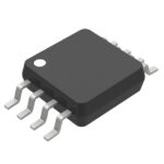 MCP6S92-E/MS
The activity of extra discounts on wholesale prices is in full swing…
Please fill in your contact information and we will send you the latest wholesale price list.





