 ChipApex | Global Electronic Components Supplier
SEARCH
Search Product
Search Post
— IC芯片 | 连接器 | 传感器 | 被动器件 —
Search productSearch post
— IC芯片 | 连接器 | 传感器 | 被动器件 —
Consult the customer manager about the wholesale price.
consultation hotline:86-132-6715-2157
email:[email protected]
Contact the product manager for consultation. One-stop consultation is available.
Do you want a lower wholesale price? Please send us your inquiry and we will reply immediately.
The MK1575-01GI is a clock recovery Phase-Locked Loop (PLL) designed for cost-sensitive video and telecom applications. It synthesizes high-frequency data or graphics pixel clocks from low-frequency reference inputs. The device operates on a single 3.3V supply with a voltage range of 3.15V to 3.45V, consuming 10mA at typical conditions. It features LVCMOS outputs and supports a maximum output frequency of 80MHz. Packaged in a 16-TSSOP, it includes selectable internal feedback dividers for standard frequencies and allows external loop filter customization for specific jitter and bandwidth requirements.
Verify the 'GI' suffix indicates the industrial temperature grade (-40°C to +85°C). Confirm RoHS compliance status as non-green parts have reached End-of-Life. Check current availability through authorized distributors since original manufacturer IDT was acquired by Renesas.
Select this component when low-cost clock synthesis from low-frequency references is required. Ensure external loop filter components are chosen to meet specific damping factor and bandwidth needs for the application. Verify that the 80MHz maximum output frequency meets system requirements.
This part belongs to the MK1575-01 family of clock recovery PLLs. The 'GI' suffix specifically denotes the industrial temperature range variant packaged in tubes. Other variants include commercial temperature ranges and lead-free options.
Direct replacements may be limited due to EOL status. Consider the MK2069 for lower jitter requirements or verify if other Renesas/IDT clock synthesizers support similar pinouts and frequency ranges.
The OE pin acts as an Output Enable. When held high, it tristates the CLK1, CLK2, and FCLK outputs and powers down the PLL.
Loop bandwidth is adjusted using external components connected to the CHGP and CHPR pins, specifically the resistor (RS) and capacitor (CS).
Yes, connecting FCLK to FBIN is the standard configuration for pre-configured frequencies without an external divider. Connecting CLK1 or CLK2 to FBIN creates a zero-delay buffer configuration.
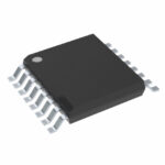 MK1575-01GI
The activity of extra discounts on wholesale prices is in full swing…
Please fill in your contact information and we will send you the latest wholesale price list.






