 ChipApex | Global Electronic Components Supplier

SEARCH
Search Product
Search Post
— IC芯片 | 连接器 | 传感器 | 被动器件 —
Search productSearch post
— IC芯片 | 连接器 | 传感器 | 被动器件 —
Consult the customer manager about the wholesale price.
consultation hotline:86-132-6715-2157
email:[email protected]
Contact the product manager for consultation. One-stop consultation is available.
Do you want a lower wholesale price? Please send us your inquiry and we will reply immediately.
The MK2069-01 is a VCXO-based clock generator providing synchronization, jitter attenuation, and frequency translation. It accepts input clocks from 1 kHz to 170 MHz and generates outputs from 500 kHz to 160 MHz. The device features a 3:1 input MUX for master/slave selection and a PLL lock status output. It operates on a single 3.3 V supply with 5 V tolerant inputs on ICLK0 and ICLK1. Packaged in a 56-pin TSSOP, it includes a CLR function for rapid phase synchronization and free-run capability without an input clock.
Verify component authenticity through authorized channels. Confirm the specific suffix 'GI' matches the required environmental compliance and package variant. Check for End-of-Life (EOL) notices regarding non-green parts as indicated in historical documentation. Ensure external loop filter components are selected to meet specific jitter attenuation and stability requirements.
Select this device when low phase noise generation is critical despite low-frequency or jittery input sources. Designers must configure external resistors and capacitors to set the VCXO PLL loop bandwidth and damping factor. Ensure the external crystal frequency falls within the 8–27 MHz range for optimal performance. Verify that the required output frequencies can be achieved using the available divider ratios.
The MK2069-01 belongs to the IDT VCXO-based line card synchronizer family. It is designed for mixed analog/digital integrated circuits where PCB layout sensitivity impacts performance. The device replaces discrete VCXO-based hybrid timing solutions to reduce cost while maintaining high performance standards for telecom and networking infrastructure.
Publicly confirmed substitute part numbers are not available in the provided source material. Evaluate alternative VCXO-based clock generators with similar input/output frequency ranges and dual PLL architectures if replacement is necessary.
The device uses the CLR (Clear) input to reset the FV Divider before reselecting the input via the MUX. This removes the memory of the previous phase, allowing the VCXO PLL to lock to the new input with minimal cycle slips and no extra clock cycles.
Jitter attenuation is determined by the VCXO PLL's low-pass frequency response, which is configured by selecting external passive components (RS, CS, CP, RSET) and setting the SV and FV divider values.
Yes, the device will free-run based on the external VCXO crystal frequency if no input clock is present. The CLR pin can also provide a short-term holdover function by keeping the charge pump inactive.
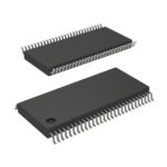 MK2069-01GI

The activity of extra discounts on wholesale prices is in full swing…
Please fill in your contact information and we will send you the latest wholesale price list.





