 ChipApex | Global Electronic Components Supplier

SEARCH
Search Product
Search Post
— IC芯片 | 连接器 | 传感器 | 被动器件 —
Search productSearch post
— IC芯片 | 连接器 | 传感器 | 被动器件 —
Consult the customer manager about the wholesale price.
consultation hotline:86-132-6715-2157
email:[email protected]
Contact the product manager for consultation. One-stop consultation is available.
Do you want a lower wholesale price? Please send us your inquiry and we will reply immediately.
The MK2732-06G is a low-cost, low-jitter VCXO and PLL clock synthesizer designed to replace discrete VCXOs and multipliers. It accepts a 0 to 3 V tuning voltage to vary output clocks by ±100 ppm using an external 10–14 MHz pullable crystal. The device provides up to three CMOS outputs with 25 mA drive capability at TTL levels. It operates on a 5 V core supply (VDD5) with configurable 3.3 V or 5 V I/O (VDDIO). Key electrical parameters include a maximum absolute jitter of ±150 ps, phase noise of -115 dBc/Hz at 10 kHz offset, and zero ppm synthesis error across all clocks.
Verify the specific suffix for the required temperature grade and packaging format. The 'G' suffix indicates lead-free composition. Suffixes 'TR' denote tape and reel shipping, while absence implies tube packaging. The 'I' suffix designates the industrial temperature version (-40°C to +85°C), whereas standard parts operate from 0°C to +70°C. Confirm current manufacturing status as non-green variants may have reached end-of-life.
Select the appropriate I/O voltage (VDDIO) based on downstream logic requirements; the core must remain at 5 V. Ensure the external crystal falls within the 10–14 MHz range and meets load capacitance specifications for optimal pullability. Use the S1/S0 pin configuration table to determine available output frequencies. Verify that the PCB layout minimizes stray capacitance near the crystal pins to maintain frequency accuracy.
This component belongs to the IDT MK27xx family of clock synthesizers, which utilize analog PLL techniques to generate precise timing signals. The MK2732-06 specifically targets applications requiring low-phase-noise VCXO functionality combined with frequency multiplication. It serves as a consolidated solution for eliminating separate VCXO, multiplier, and buffer components from the board design.
Public confirmed substitute part numbers are not provided in the source material.
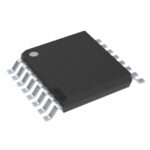 MK2732-06G

The activity of extra discounts on wholesale prices is in full swing…
Please fill in your contact information and we will send you the latest wholesale price list.





