 ChipApex | Global Electronic Components Supplier
SEARCH
Search Product
Search Post
— IC芯片 | 连接器 | 传感器 | 被动器件 —
Search productSearch post
— IC芯片 | 连接器 | 传感器 | 被动器件 —
Consult the customer manager about the wholesale price.
consultation hotline:86-132-6715-2157
email:[email protected]
Contact the product manager for consultation. One-stop consultation is available.
Do you want a lower wholesale price? Please send us your inquiry and we will reply immediately.
The MPA4609IPFBR is a quad, differential I/O, 2x1 multiplexed high gain preamplifier manufactured by Texas Instruments. It features four differential output channels and two sets of four differential inputs controlled by TTL/CMOS channel select lines. The device operates on a single +5V supply with a quiescent current of 50mA. It provides a nominal open-load gain of 190V/V and a bandwidth of 90MHz up to a 3.5Vpp output. Key electrical characteristics include a low input noise voltage of 0.65nV/√Hz, a differential slew rate of 150V/µs, and an operating temperature range from -40°C to +85°C.
Verify the package designator PFB corresponds to the TQFP-48 form factor required for your PCB layout. Confirm the suffix BR indicates the tape and reel packaging format with a quantity of 2000 units. Ensure the operating temperature grade supports environments ranging from -40°C to +85°C. Cross-reference the ordering number MPA4609IPFBR against the latest manufacturer documentation to validate current production status and availability.
Select this component when a fixed high gain of approximately 190V/V is required for differential signal conditioning. It is suitable for applications demanding low input noise voltage below 1nV/√Hz and wide bandwidth exceeding 90MHz. The device is appropriate for systems requiring multiplexing between two input sources using simple digital control lines. Consider its single +5V supply operation and low quiescent current for power-constrained multi-channel designs.
The MPA4609 belongs to a family of fixed-gain differential amplifiers designed for low-level signal amplification. It integrates multiple amplifier stages into a single chip to reduce board space and component count. The device is optimized for high-speed data acquisition and audio processing applications where maintaining signal integrity across multiple channels is critical.
No public confirmed substitute part numbers are available in the provided documentation.
Channel selection is managed by two TTL/CMOS compatible pins (Pin 3 and Pin 34). A voltage below 0.9V selects the reverse channels, while a voltage above 1.6V selects the forward channels.
The maximum no-load differential output swing is 3.5Vpp, centered on the 2.1V internal bias level.
The nominal gain of 190V/V can be reduced by adding an external load resistor between the differential output pins. For example, a 940Ω resistor reduces the gain by half to 95V/V.
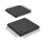 MPA4609IPFBR
The activity of extra discounts on wholesale prices is in full swing…
Please fill in your contact information and we will send you the latest wholesale price list.





