 ChipApex | Global Electronic Components Supplier

SEARCH
Search Product
Search Post
— IC芯片 | 连接器 | 传感器 | 被动器件 —
Search productSearch post
— IC芯片 | 连接器 | 传感器 | 被动器件 —
Consult the customer manager about the wholesale price.
consultation hotline:86-132-6715-2157
email:[email protected]
Contact the product manager for consultation. One-stop consultation is available.
Do you want a lower wholesale price? Please send us your inquiry and we will reply immediately.
MPC905DR2 is listed in the Clock Buffers, Drivers range at ChipApex. The manufacturer field lists NXP USA Inc.. Its product description is IC CLK BUFFER 1:6 100MHZ 16SOIC. Review the specifications below when checking this part for your BOM.
The MPC905 is a six-output clock generation and fanout buffer device designed for PCI bus environments operating at 3.3V or 5.0V. It accepts an external crystal or TTL-compatible clock input and generates six low-skew LVCMOS outputs (BCLK0–BCLK5). The device operates from a 3.3V supply with 5.0V tolerant inputs, supporting maximum frequencies of 50 MHz with crystals and 100 MHz with external sources. Each output can drive up to two series-terminated 50 Ω transmission lines, providing a 1:12 fanout capability.
Verify the package suffix 'D' corresponds to the 16-lead Plastic SOIC (Case 751B-05). Confirm the operating temperature range matches the application requirements, as the datasheet specifies 0°C to +70°C. Ensure the supply voltage remains within the functional range of 3.0V to 3.6V. Check for any ordering suffixes that may indicate tape-and-reel packaging versus tubes, though the document primarily references the D suffix.
Select the MPC905 when a single source must distribute clocks to multiple loads (up to 12) in a PCI architecture. It is suitable for designs requiring independent control of the main clock group (BCLK0–4) and the block clock (BCLK5) for power saving. Ensure the external crystal meets the specified ESR (50–80Ω) and shunt capacitance (5–7pF) for reliable oscillation at 33.3333 MHz or 11.1111 MHz.
The MPC905 was originally manufactured by Motorola Semiconductor Products Inc., which later became NXP Semiconductors. It serves as a specialized timing solution for legacy PCI systems. The device is distinct from general-purpose clock buffers due to its integrated oscillator interface and specific synchronization features tailored for bus standards.
Publicly confirmed substitute part numbers are not available in the provided documentation. Designers should consult current NXP product portfolios for modern replacements, ensuring compatibility with LVCMOS levels and pin configurations if direct replacement is required.
Both enable inputs are synchronized internally to ensure output disabling occurs only when outputs are already LOW, preventing runt pulses. Enable1 pulls BCLK0–BCLK4 low, while Enable2 pulls BCLK5 low. The oscillator continues running during these states.
Each output has an approximate impedance of 10 Ω and can drive either one parallel-terminated 50 Ω line or two series-terminated 50 Ω lines. Series termination allows for higher fanout without DC current draw.
For fundamental mode (33.3333 MHz), use an AT-cut crystal with 5–7 pF shunt capacitance and 50–80 Ω ESR. For third overtone (11.1111 MHz), additional trap components (CTRAP, LTRAP) are required as shown in Figure 2.
Explore related parts through Clock/Timing, Integrated Circuits (ICs), all product categories, ChipApex homepage.
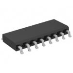 MPC905DR2

The activity of extra discounts on wholesale prices is in full swing…
Please fill in your contact information and we will send you the latest wholesale price list.





