 ChipApex | Global Electronic Components Supplier
SEARCH
Search Product
Search Post
— IC芯片 | 连接器 | 传感器 | 被动器件 —
Search productSearch post
— IC芯片 | 连接器 | 传感器 | 被动器件 —
Consult the customer manager about the wholesale price.
consultation hotline:86-132-6715-2157
email:[email protected]
Contact the product manager for consultation. One-stop consultation is available.
Do you want a lower wholesale price? Please send us your inquiry and we will reply immediately.
The MPC9109 is a low voltage 1:18 clock distribution chip designed for synchronous systems. It accepts either differential LVPECL or single-ended LVCMOS inputs and provides 18 LVCMOS outputs compatible with 2.5 V or 3.3 V logic levels. The device supports maximum input frequencies of up to 250 MHz at 3.3 V operation, with output-to-output skew limited to 200 ps. It features an output impedance of approximately 20 Ω, enabling the drive of series terminated transmission lines. The component operates within a supply voltage range of 2.375 V to 3.465 V and is housed in a 32-lead LQFP package.
Verify the specific ordering suffix (FA or AC) to confirm lead-free status and exact voltage configuration requirements. Confirm that the 32-LQFP (7x7 mm) package dimensions align with the target PCB footprint. Ensure the design environment supports the required 2.5 V or 3.3 V core and output supply voltages as specified in the electrical characteristics tables.
Select this component when a 1:18 fanout is required with low skew specifications. Choose the FA suffix for standard packaging or AC suffix for Pb-free availability. Verify compatibility between the source clock signal (LVPECL vs LVCMOS) and the LVCMOS_CLK_Sel pin configuration. Ensure the target system voltage matches the available VCCI and VCCO supply options.
The MPC9109 belongs to the Advanced Clock Drivers Devices family from Freescale Semiconductor, now part of NXP USA Inc. It serves as a mid-performance solution compared to higher-speed variants like the MPC940L or lower-impedance drivers like the MPC942. The device was originally manufactured under the Freescale brand before corporate integration.
For higher performance requirements, consult the MPC940L data sheet. For lower output impedance needs, refer to the MPC942 data sheet. Direct functional substitutes are not explicitly listed in the provided documentation.
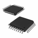 MPC9109FA
The activity of extra discounts on wholesale prices is in full swing…
Please fill in your contact information and we will send you the latest wholesale price list.






