 ChipApex | Global Electronic Components Supplier

SEARCH
Search Product
Search Post
— IC芯片 | 连接器 | 传感器 | 被动器件 —
Search productSearch post
— IC芯片 | 连接器 | 传感器 | 被动器件 —
Consult the customer manager about the wholesale price.
consultation hotline:86-132-6715-2157
email:[email protected]
Contact the product manager for consultation. One-stop consultation is available.
Do you want a lower wholesale price? Please send us your inquiry and we will reply immediately.
The MPC9315 is a 2.5 V and 3.3 V compatible, PLL-based clock generator designed for low-skew clock distribution in telecom, networking, and computing applications. It features eight LVCMOS outputs divided into three banks (A, B, C) and two selectable reference inputs for redundancy. The device supports configurable output-to-input frequency ratios of 1:1, 2:1, 4:1, 1:2, and 1:4. A fully integrated PLL eliminates the need for external loop filter components. The internal VCO operates between 75 MHz and 160 MHz, enabling output frequencies from 18.75 MHz to 160 MHz. Maximum output skew is 120 ps across any output and 80 ps within a single bank.
Verify package suffixes against ordering information. The FA suffix denotes a standard 32-lead LQFP package. The AC suffix indicates a Pb-free version of the same 32-lead LQFP package. Confirm RoHS compliance status based on the specific suffix ordered, as general product descriptions may not reflect individual lot certifications.
Select the MPC9315 when zero-delay buffer operation or precise phase alignment is required. Ensure the feedback path connects an output to FB0 or FB1 to close the PLL loop. Use FSELA, FSELB, and FSELC pins to configure divider ratios per output bank. For noise-sensitive designs, implement the recommended RC filter on the VCCA pin to isolate the analog PLL supply from digital switching noise.
Manufactured by Freescale Semiconductor (now NXP), this component belongs to the Advanced Clock Drivers Devices family. It is specifically engineered for low-voltage CMOS environments, offering compatibility with microprocessors such as PowerQUICC I and II. The device replaces older discrete clock distribution solutions by integrating the PLL and output buffers into a single 32-lead LQFP package.
Public confirmed substitute part numbers are not available in the provided documentation.
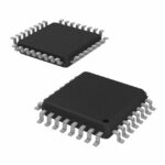 MPC9315FA

The activity of extra discounts on wholesale prices is in full swing…
Please fill in your contact information and we will send you the latest wholesale price list.





