 ChipApex | Global Electronic Components Supplier

SEARCH
Search Product
Search Post
— IC芯片 | 连接器 | 传感器 | 被动器件 —
Search productSearch post
— IC芯片 | 连接器 | 传感器 | 被动器件 —
Consult the customer manager about the wholesale price.
consultation hotline:86-132-6715-2157
email:[email protected]
Contact the product manager for consultation. One-stop consultation is available.
Do you want a lower wholesale price? Please send us your inquiry and we will reply immediately.
The MPC9600FA is a low voltage 2.5 V or 3.3 V compatible, 1:21 PLL-based clock driver and fanout buffer manufactured by NXP USA Inc. (formerly Motorola). It features an integrated phase-locked loop capable of multiplying input frequencies by 2, 3, 4, or 6 to generate output frequencies up to 200 MHz. The device provides 21 LVCMOS outputs organized into three selectable banks (QA, QB, QC) with maximum output-to-output skew of 150 ps and cycle-to-cycle jitter of ±50 ps. It accepts LVPECL or LVCMOS reference clocks and operates within a temperature range of -40°C to +85°C in a 48-lead LQFP package.
Verify the specific suffix 'FA' corresponds to the 48-lead LQFP package variant when sourcing. Confirm that the component meets the required operating temperature range of -40°C to +85°C for the intended environment. Ensure power supply filtering on the VCCA pin is implemented according to datasheet recommendations to maintain PLL stability and minimize jitter.
Select this component when a single source must drive multiple loads with tight skew requirements. The device supports input frequencies from 16.67 MHz to 50 MHz. Designers must ensure the VCO frequency remains between 200 MHz and 400 MHz for stable operation. Consider the separate VCC and VCCA power pins; a filter circuit on VCCA is recommended to isolate analog PLL noise from digital switching noise.
The MPC9600 is part of the Motorola/NXP timing solutions family designed for low-voltage CMOS applications. It serves as a bridge between high-speed differential clock sources and LVCMOS logic loads. The device replaces older discrete PLL and buffer combinations by integrating the feedback path and output drivers into a single 48-pin package.
Public confirmed substitute part numbers are not available in the provided documentation.
It uses an external feedback path where the QFB output is connected to the FB_IN input. The internal PLL aligns the feedback clock edge with the reference clock input edge, virtually eliminating propagation delay.
VCCA supplies the analog PLL circuitry. Driving VCCA to GND bypasses the PLL for static testing. A power supply filter is recommended on this pin to reduce jitter caused by system noise.
Yes. While each output can drive one parallel terminated line, it can drive up to two series terminated lines per output, effectively doubling the total fanout capability to 1:42.
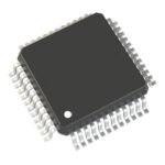 MPC9600FA

The activity of extra discounts on wholesale prices is in full swing…
Please fill in your contact information and we will send you the latest wholesale price list.





