 ChipApex | Global Electronic Components Supplier

SEARCH
Search Product
Search Post
— IC芯片 | 连接器 | 传感器 | 被动器件 —
Search productSearch post
— IC芯片 | 连接器 | 传感器 | 被动器件 —
Consult the customer manager about the wholesale price.
consultation hotline:86-132-6715-2157
email:[email protected]
Contact the product manager for consultation. One-stop consultation is available.
Do you want a lower wholesale price? Please send us your inquiry and we will reply immediately.
The MPC9608 is a 3.3 V compatible, 1:10 PLL-based zero-delay clock buffer manufactured by Freescale Semiconductor (NXP). It features a single reference clock input and two banks of five LVCMOS outputs. The device supports an I/O frequency range of 12.5 to 200 MHz with selectable divide-by-two for one output bank. It operates on a single 3.3 V supply within an ambient temperature range of -40 °C to +85 °C. Packaged in a 7x7 mm² 32-lead LQFP, it provides low output skew and synchronous enable control.
Verify the ordering suffix against the package type. The 'FA' suffix indicates a standard 32-lead LQFP package, while the 'AC' suffix denotes a lead-free version of the same 32-lead LQFP package. Confirm the specific suffix requirement matches the intended manufacturing process before procurement.
Select this component for nested clock tree designs requiring near-zero insertion delay. Ensure the system requires a 3.3 V supply and LVCMOS compatibility. Verify that the required frequency falls within the 12.5–200 MHz range defined by the F_RANGE pins. Consider the separate VCCA power supply filtering requirements for optimal jitter performance.
This device belongs to the Advanced Clock Drivers family from Freescale Semiconductor. It is designed as a fanout buffer to replace traditional CMOS buffers, offering significantly lower clock skew through its PLL-based zero-delay architecture. It targets mid-range clock distribution in high-performance digital systems.
Publicly confirmed substitute part numbers are not available in the provided documentation.
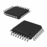 MPC9608FA

The activity of extra discounts on wholesale prices is in full swing…
Please fill in your contact information and we will send you the latest wholesale price list.





