 ChipApex | Global Electronic Components Supplier

SEARCH
Search Product
Search Post
— IC芯片 | 连接器 | 传感器 | 被动器件 —
Search productSearch post
— IC芯片 | 连接器 | 传感器 | 被动器件 —
Consult the customer manager about the wholesale price.
consultation hotline:86-132-6715-2157
email:[email protected]
Contact the product manager for consultation. One-stop consultation is available.
Do you want a lower wholesale price? Please send us your inquiry and we will reply immediately.
The MPC961C is a 2.5V or 3.3V compatible, 1:18 PLL-based zero-delay buffer designed for demanding clock tree applications. It features fully integrated PLL circuitry with LVCMOS outputs capable of frequencies up to 200MHz. The device provides output skews of 150ps and cycle-to-cycle jitter of ±50ps RMS. It accepts an LVCMOS reference clock via the CCLK pin and requires an external RC filter on the VCCA analog power supply pin. Packaged in a 32-lead LQFP (CASE 873A-02), it supports series or parallel terminated transmission lines.
Verify the specific ordering suffix against the manufacturer's current product status. Confirm that the required external RC filter components for the VCCA pin are included in the system design. Ensure the PCB layout accommodates the 32-lead LQFP package dimensions specified in CASE 873A-02.
Select the MPC961C when an LVCMOS reference clock input is required; the MPC961P variant utilizes an LVPECL reference. Designers must account for the separate VCCA power supply requirement and implement the recommended filtering to isolate analog PLL noise from digital switching activity.
Originally manufactured by Motorola Semiconductor Products Inc., this component was later transitioned to Freescale Semiconductor following corporate restructuring. The datasheet DL207 documents the technical specifications for this timing solution within the broader portfolio of clock distribution devices.
The MPC961P serves as a functional alternative within the same family but utilizes an LVPECL reference clock input instead of LVCMOS. Verify interface compatibility before substitution.
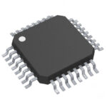 MPC961CFA

The activity of extra discounts on wholesale prices is in full swing…
Please fill in your contact information and we will send you the latest wholesale price list.






