 ChipApex | Global Electronic Components Supplier
SEARCH
Search Product
Search Post
— IC芯片 | 连接器 | 传感器 | 被动器件 —
Search productSearch post
— IC芯片 | 连接器 | 传感器 | 被动器件 —
Consult the customer manager about the wholesale price.
consultation hotline:86-132-6715-2157
email:[email protected]
Contact the product manager for consultation. One-stop consultation is available.
Do you want a lower wholesale price? Please send us your inquiry and we will reply immediately.
The MPC9817ENR2 is a PLL-based clock generator designed for PowerQUICC and PowerPC microprocessor applications. It generates system clocks at selectable frequencies of 25, 33, 50, or 66 MHz using a 25 MHz reference input from an external source or on-chip crystal oscillator. The device provides five LVCMOS processor outputs and three buffered 25 MHz reference outputs. Operating with a 3.3V supply within the -40°C to +85°C temperature range, it features low cycle-to-cycle jitter (150 ps) and output skew (100 ps). Packaged in a 20-lead SSOP, it supports computing, networking, and telecommunications environments.
Verify component authenticity as the original manufacturer, Freescale Semiconductor, was acquired by Integrated Device Technology (IDT), which was subsequently acquired by Renesas Electronics Corporation. Confirm that the EN suffix indicates a lead-free package variant compatible with RoHS standards. Ensure the 20-SSOP package dimensions match the CASE 1461-01 specification during mechanical integration.
Select this component when designing systems requiring specific PCI bus frequencies (33/66 MHz) for Power architecture processors. The device requires a 25 MHz reference; ensure the design accommodates either an external 25 MHz signal or a 25 MHz crystal with CL=10 pF load capacitance. Verify that the 3.3V ±5% supply voltage aligns with the system power rails and that the LVCMOS output drive strength meets the fan-out requirements of the target logic.
The MPC9817 belongs to the IDT NetCOM family of advanced clock drivers originally developed by Freescale Semiconductor's Timing Solutions Organization. Following corporate acquisitions, intellectual property rights transferred through IDT to Renesas Electronics Corporation. This part represents a specialized timing solution for legacy embedded processing architectures rather than general-purpose consumer electronics.
Direct functional replacements are limited due to proprietary frequency synthesis configurations. Review current Renesas timing portfolios for similar PLL-based generators if redesigning. Cross-reference with IDT legacy part numbers to identify pin-compatible alternatives, noting that newer generations may offer differential outputs or lower jitter specifications not present in this single-ended LVCMOS device.
The output frequency is set by the logic levels on the FSEL0 and FSEL1 pins. Configurations yield 25 MHz (both low), 33 MHz (FSEL0 low, FSEL1 high), 50 MHz (FSEL0 high, FSEL1 low), or 66 MHz (both high).
The device supports a 25 MHz AT-cut parallel resonant crystal with a load capacitance (CL) of 10 pF. No additional external capacitors are required, though they may be added to XTAL_IN/OUT for fine-tuning.
Yes. An external 25 MHz reference can be applied to the XTAL_IN pin. In this mode, the XTAL_OUT pin must be left floating to disable the internal oscillator.
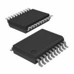 MPC9817ENR2
The activity of extra discounts on wholesale prices is in full swing…
Please fill in your contact information and we will send you the latest wholesale price list.






