ChipApex | Global Electronic Components Supplier
SEARCH
Search Product
Search Post
— IC芯片 | 连接器 | 传感器 | 被动器件 —
Search productSearch post
— IC芯片 | 连接器 | 传感器 | 被动器件 —
Consult the customer manager about the wholesale price.
consultation hotline:86-132-6715-2157
email:[email protected]
Contact the product manager for consultation. One-stop consultation is available.
Do you want a lower wholesale price? Please send us your inquiry and we will reply immediately.
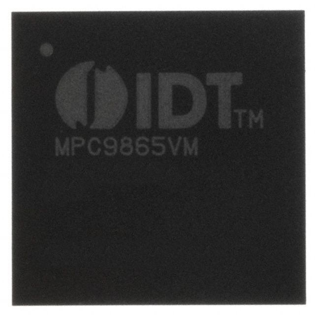
The MPC9865VM is a PLL-based clock generator designed for PowerQUICC III and PowerPC microprocessor applications. It features an internal oscillator or external reference input (25/33 MHz) to generate up to eight LVCMOS outputs across two configurable banks. The device supports output frequencies ranging from 16 MHz to 200 MHz, derived from a 2 GHz VCO. It operates on a 3.3V supply with LVCMOS outputs at 3.3V or 2.5V. Key specifications include low cycle-to-cycle jitter (150 ps max), low output skew (50 ps within bank), and an operating temperature range of -40°C to +85°C. The component is housed in a 100-lead MAPBGA package.
Verify the specific suffix 'VM' indicates the lead-free PB-free package variant as per the datasheet. Confirm that the source document identifies the manufacturer as Freescale Semiconductor or IDT, noting the acquisition history. Ensure the part status is checked against current availability as the device may be obsolete.
Select this component when designing systems requiring precise clock generation for PowerQUICC or PowerPC processors. Ensure the design accommodates the 100-lead MAPBGA footprint. Verify that the required output frequencies align with the supported dividers (N=8 to 126) and that the 3.3V core supply voltage matches the system power rails.
The MPC9865 series was originally developed by Freescale Semiconductor for networking and telecom applications. Following corporate restructuring, the timing solutions organization was acquired by Integrated Device Technology (IDT). The datasheet reflects this transition, often listing both entities. This specific model serves as a dedicated clock generator for high-performance embedded processors.
Consult official cross-reference lists from IDT or Renesas for direct replacements. Generic clock generators may not support the specific configuration pins (CLK_A, CLK_B) or frequency ranges required for PowerQUICC compatibility without hardware modifications.
Output frequencies are configured using six control pins per bank (CLK_A and CLK_B). These pins set the division factor N, where the output frequency is calculated as fout = 2000 / N MHz.
The device supports a 25 MHz crystal oscillator via XTAL_IN/OUT, or external reference clocks of 25 MHz or 33 MHz. External inputs can be single-ended LVCMOS or differential LVPECL.
The maximum cycle-to-cycle jitter (tJIT(CC)) is specified as 150 ps under standard operating conditions (TA = –40°C to +85°C).
 MPC9865VM
The activity of extra discounts on wholesale prices is in full swing…
Please fill in your contact information and we will send you the latest wholesale price list.