ChipApex | Global Electronic Components Supplier
SEARCH
Search Product
Search Post
— IC芯片 | 连接器 | 传感器 | 被动器件 —
Search productSearch post
— IC芯片 | 连接器 | 传感器 | 被动器件 —
Consult the customer manager about the wholesale price.
consultation hotline:86-132-6715-2157
email:[email protected]
Contact the product manager for consultation. One-stop consultation is available.
Do you want a lower wholesale price? Please send us your inquiry and we will reply immediately.
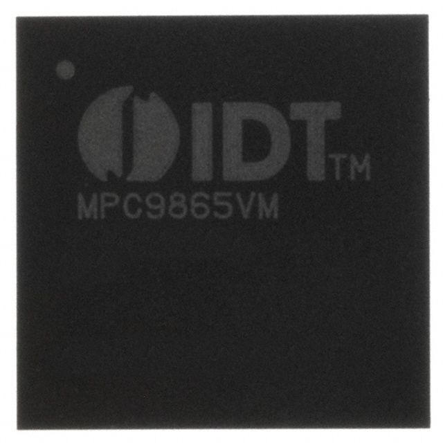
The MPC9865VMR2 is a PLL-based clock generator designed for PowerQUICC III microprocessor applications. It generates eight low-skew LVCMOS outputs across two configurable banks, supporting frequencies from 16 MHz to 200 MHz derived from a 2 GHz internal VCO. The device accepts 25 MHz or 33 MHz reference inputs via crystal or external sources (LVCMOS/LVPECL). Operating on a 3.3 V supply with an extended temperature range of -40°C to +85°C, it utilizes a 100-lead CABGA package.
Verify component status as the MPC9865 series has reached End-of-Life (EOL) per manufacturer notices dated February 2016. Confirm availability through authorized distributors or secondary markets. Ensure the VM suffix indicates Pb-free packaging compatible with current assembly processes. Validate pinout compatibility during replacement planning.
Select this component when designing systems requiring specific PowerPC/PowerQUICC bus frequencies. Ensure the design accommodates the 3.3 V core supply and optional 2.5 V or 3.3 V output supplies. Verify that the required output frequencies align with the available division ratios (N=8 to 126). Consider the 100-lead MAPBGA footprint constraints during PCB layout.
Originally manufactured by Freescale Semiconductor, the MPC9865 was acquired by Integrated Device Technology (IDT) and subsequently by Renesas Electronics Corporation. The part number suffix 'VM' denotes the lead-free variant housed in a 100-lead MAPBGA package. This device belongs to the NETCOM family of advanced clock drivers optimized for networking and telecom infrastructure.
Public confirmed substitute part numbers are not provided in the source material. Due to the EOL status, engineers should evaluate newer Renesas VersaClock or FemtoClock families for functional equivalents, ensuring voltage levels and package dimensions match the existing design.
The maximum output frequency is 200 MHz, achieved by dividing the 2000 MHz VCO frequency by a factor of 10.
Yes, the device supports differential LVPECL inputs on pins PCLK and PCLK, in addition to single-ended LVCMOS and crystal inputs.
Output frequencies are configured using digital control pins CLK_A and CLK_B, which set the division ratio N for Bank A and Bank B respectively.
 MPC9865VMR2
The activity of extra discounts on wholesale prices is in full swing…
Please fill in your contact information and we will send you the latest wholesale price list.