 ChipApex | Global Electronic Components Supplier

SEARCH
Search Product
Search Post
— IC芯片 | 连接器 | 传感器 | 被动器件 —
Search productSearch post
— IC芯片 | 连接器 | 传感器 | 被动器件 —
Consult the customer manager about the wholesale price.
consultation hotline:86-132-6715-2157
email:[email protected]
Contact the product manager for consultation. One-stop consultation is available.
Do you want a lower wholesale price? Please send us your inquiry and we will reply immediately.
The MPC9893AE is a 2.5 V and 3.3 V compatible, PLL-based intelligent dynamic clock switch and generator designed for redundant clock distribution systems. It accepts two LVCMOS reference clock inputs and generates 12 phase-aligned outputs organized into two banks. The device features an on-chip Intelligent Dynamic Clock Switch (IDCS) that automatically detects failing reference clocks and switches to a redundant signal without output interruption or phase bumps. Operating within a frequency range of 7.5 MHz to 200 MHz, it provides low skew characteristics with a maximum output-to-output skew of 50 ps within a bank.
Verify the specific suffix 'AE' corresponds to the 48-lead Pb-free LQFP package (Case 932-03). Confirm ambient operating temperature range is -40 °C to 85 °C. Ensure power supply filtering is implemented on the VCC_PLL pin using an RC filter to isolate analog noise, as specified in the application guidelines.
Select this component when designing systems requiring automatic redundancy switching between two clock sources. Verify that the required output frequency falls within the 7.5–200 MHz range. Consider the internal VCO frequency and PLL feedback divider configuration if minimizing I/O jitter is critical for the specific application timing constraints.
The MPC9893 belongs to the Advanced Clock Drivers family from Freescale Semiconductor. It is specifically engineered for applications demanding high reliability and precise timing synchronization. The device integrates both digital logic for clock switching and analog PLL circuitry to maintain signal integrity across varying load conditions.
Publicly confirmed substitute part numbers are not available in the provided documentation. Evaluate alternative clock generators based on LVCMOS compatibility, IDCS functionality, and package dimensions (48-lead LQFP).
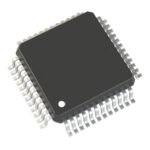 MPC9893AE

The activity of extra discounts on wholesale prices is in full swing…
Please fill in your contact information and we will send you the latest wholesale price list.





