 ChipApex | Global Electronic Components Supplier

SEARCH
Search Product
Search Post
— IC芯片 | 连接器 | 传感器 | 被动器件 —
Search productSearch post
— IC芯片 | 连接器 | 传感器 | 被动器件 —
Consult the customer manager about the wholesale price.
consultation hotline:86-132-6715-2157
email:[email protected]
Contact the product manager for consultation. One-stop consultation is available.
Do you want a lower wholesale price? Please send us your inquiry and we will reply immediately.
The MPC99J93FA is a PLL clock driver and Intelligent Dynamic Clock Switch (IDCS) manufactured by NXP USA Inc. It accepts two differential LVPECL input signals and generates five new differential LVPECL outputs. Two output pairs regenerate the input frequency and phase, while three pairs generate 2x phase-aligned outputs. The device operates on a 3.3V supply with an input reference frequency range of 50 MHz to 90 MHz and a VCO frequency range of 200 MHz to 360 MHz. It features LVCMOS control I/O and is housed in a 32-lead LQFP package.
Verify that the FA suffix corresponds to the standard 32-lead LQFP package as defined in the Freescale Semiconductor datasheet Rev 3. Confirm that the component source matches the original manufacturer specifications for the MPC99J93 series. Ensure compatibility with 3.3V operation and LVPECL signal levels required by the target application circuitry.
Select this component when designing redundant clock architectures requiring automatic failover between two LVPECL sources. The device supports a maximum output frequency of 180 MHz on the 2x outputs. Ensure the system design accommodates the specified thermal resistance values and provides proper termination voltage (VTT = VCC - 2V) for the LVPECL outputs to maintain AC characteristics.
The MPC99J93 is part of the Advanced Clock Drivers Devices family originally released by Freescale Semiconductor. The 'FA' suffix indicates the specific 32-lead LQFP packaging variant. This component is designed to eliminate typical phase bumps during clock failure events by continuously monitoring input signals and switching to a secondary clock source seamlessly.
Public confirmed substitute part numbers are not available in the provided documentation.
The IDCS continuously monitors both input CLK signals. Upon detecting a failure (CLK stuck HIGH or LOW for at least one period), it latches the INP_BAD flag and switches to the good secondary clock, performing phase/frequency alignment with minimal output phase disturbance.
The Qb0:2 output pairs generate 2x, phase-aligned clock outputs derived from the selected input reference signal.
The absolute maximum continuous rating for the VCC Supply Voltage is -0.3 V to 3.9 V.
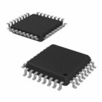 MPC99J93FA

The activity of extra discounts on wholesale prices is in full swing…
Please fill in your contact information and we will send you the latest wholesale price list.






