ChipApex | Global Electronic Components Supplier
SEARCH
Search Product
Search Post
— IC芯片 | 连接器 | 传感器 | 被动器件 —
Search productSearch post
— IC芯片 | 连接器 | 传感器 | 被动器件 —
Consult the customer manager about the wholesale price.
consultation hotline:86-132-6715-2157
email:[email protected]
Contact the product manager for consultation. One-stop consultation is available.
Do you want a lower wholesale price? Please send us your inquiry and we will reply immediately.
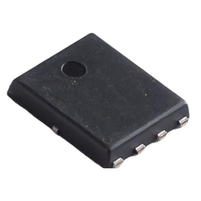
The MSH80N087AU is an N-Channel MOSFET utilizing trench DMOS technology, designed for high-efficiency fast switching applications. It features a Drain-Source Voltage (VDS) of 80 V and a Gate-Source Voltage (VGS) of ±20 V. The device guarantees a maximum static Drain-Source On-Resistance (RDS(on)) of 8.7 mΩ at VGS =10V and 13 mΩ at VGS =4.5V. Continuous Drain Current (ID) reaches 60 A at TC=25°C and 38 A at TC=100°C, with a Pulsed Drain Current (IDM) of 170 A. Power Dissipation (PD) is rated at 52 W at TC=25°C. Operating Junction Temperature ranges from -55 to 175 °C.
Verify the specific datasheet revision against the manufacturer's official documentation before finalizing procurement. Confirm that the PDFN 5X6 package dimensions align with your PCB footprint design. Ensure thermal management strategies account for the specified junction-to-ambient resistance values under actual operating conditions. Validate component authenticity through authorized distribution channels.
Select this component for designs requiring robust avalanche energy handling and low conduction losses. Evaluate the thermal impedance characteristics relative to the expected ambient temperature and copper board area. Consider the gate charge specifications when designing drive circuits for optimal switching speed. Verify that the voltage and current ratings provide adequate margins for peak transient loads in the target application.
This component belongs to the family of surface-mount N-Channel MOSFETs produced by Bruckewell Technology Corporation. It is specifically engineered using trench DMOS architecture to deliver superior performance in power conversion and switching environments. The device is packaged in a compact form factor suitable for automated surface mount assembly processes.
No public confirmed substitute part numbers are available in the provided documentation.
The device guarantees a minimum Single Pulse Avalanche Energy of 11 mJ under test conditions of VDD=50V, L=0.1mH, and IAS=15A.
The maximum RDS(on) is specified as 8.7 mΩ at VGS=10V and increases to a maximum of 13 mΩ at VGS=4.5V, both measured at ID=10A.
 MSH80N087AU
The activity of extra discounts on wholesale prices is in full swing…
Please fill in your contact information and we will send you the latest wholesale price list.