 ChipApex | Global Electronic Components Supplier

SEARCH
Search Product
Search Post
— IC芯片 | 连接器 | 传感器 | 被动器件 —
Search productSearch post
— IC芯片 | 连接器 | 传感器 | 被动器件 —
Consult the customer manager about the wholesale price.
consultation hotline:86-132-6715-2157
email:[email protected]
Contact the product manager for consultation. One-stop consultation is available.
Do you want a lower wholesale price? Please send us your inquiry and we will reply immediately.
N74F299D,623 is listed in the Shift Registers range at ChipApex. The manufacturer field lists NXP USA Inc.. Its product description is IC SHIFT REGISTER 8BIT 20SOIC. Review the specifications below when checking this part for your BOM.
The N74F299D,623 is an 8-bit universal shift/storage register with 3-State outputs manufactured by NXP USA Inc. It operates within a supply voltage range of 4.5V to 5.5V and supports a commercial temperature range of 0°C to +70°C. The device features four operating modes: shift left, shift right, parallel load, and hold. It utilizes a 20-pin plastic Small Outline Package (SOT163-1). Key electrical characteristics include a maximum clock frequency of 115 MHz for Qn outputs and propagation delays ranging from 3.5ns to 10.5ns depending on the signal path.
Verify component authenticity through authorized distribution channels. Confirm RoHS compliance status as specified in official documentation. Check for obsolescence notices or lifecycle changes prior to finalizing procurement plans. Ensure packaging specifications match system assembly requirements.
Select this component when an 8-bit shift register with multiplexed I/O is required. Consider the 3-State output capability for bus sharing applications. Evaluate the 115 MHz maximum clock frequency against system timing requirements. Verify that the 20-pin SO package fits the available PCB footprint constraints.
This part belongs to the 74F logic family, known for high-speed performance compared to standard TTL. The N74F299D variant specifically provides universal shift and storage functionality. It serves as a digital logic building block for data manipulation tasks in industrial and consumer electronic designs.
Check for direct pin-compatible alternatives within the same logic family. Verify that substitute components maintain identical 3-State output characteristics and operating voltage ranges. Ensure functional equivalence for all four operating modes before implementation.
Explore related parts through Logic, Integrated Circuits (ICs), all product categories, ChipApex homepage.
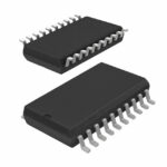 N74F299D,623

The activity of extra discounts on wholesale prices is in full swing…
Please fill in your contact information and we will send you the latest wholesale price list.





