 ChipApex | Global Electronic Components Supplier

SEARCH
Search Product
Search Post
— IC芯片 | 连接器 | 传感器 | 被动器件 —
Search productSearch post
— IC芯片 | 连接器 | 传感器 | 被动器件 —
Consult the customer manager about the wholesale price.
consultation hotline:86-132-6715-2157
email:[email protected]
Contact the product manager for consultation. One-stop consultation is available.
Do you want a lower wholesale price? Please send us your inquiry and we will reply immediately.
NB100EP223FAG is listed in the Clock Buffers, Drivers range at ChipApex. The manufacturer field lists onsemi. Its product description is IC CLK BUFFER 2:22 500MHZ 64LQFP. Review the specifications below when checking this part for your BOM.
The NB100EP223 is a low skew 1-to-22 differential clock driver designed for high-speed clock distribution. It accepts two differential clock sources (HSTL or LVPECL) via an input multiplexer controlled by an LVTTL CLK_SEL pin. The device provides 22 HSTL-compatible differential outputs, each terminated with 50 ohms to ground. Operating at VCC = 3.0V to 3.6V and VCCO = 1.6V to 2.0V, it supports frequencies exceeding 500 MHz. Key electrical parameters include a typical propagation delay of 1 ns, within-device skew of 25 ps, and device-to-device skew of 100 ps. The synchronous Output Enable (OE) prevents runt pulses.
Verify the specific ordering suffix against the datasheet table on page 9. The 'G' suffix indicates a Pb-Free package, while 'R2' denotes Tape & Reel shipping (1500 units). Standard trays contain 160 units. Confirm moisture sensitivity levels (Level 2 for Pb, Level 3 for Pb-Free) if long-term storage or reflow soldering profiles are critical to the manufacturing process.
Select this component when driving over 20 loads with strict skew requirements. Ensure the input source matches the selected mode: LVDS inputs require an external 100 ohm termination resistor across the differential pair. Verify that the PCB layout accommodates the thermal via array (4x4 grid, 1.2 mm pitch) recommended for the exposed pad to maintain junction temperatures within the 0°C to +85°C operating range.
This part belongs to the NB100EP series from ON Semiconductor's ECLinPS family. It serves as a high-fanout buffer specifically optimized for HSTL output standards while accepting legacy LVPECL or modern LVDS/HSTL inputs. It replaces older discrete fanout buffer solutions in dense digital systems.
Direct functional replacements within the same family include the NB100EP221 (1-to-5 fanout) or NB100EP222 (1-to-11 fanout) if fewer outputs are required. For higher fanout needs, verify compatibility with the NB100EP224. Pinouts differ significantly between these variants; do not assume pin-compatible substitution without reviewing the specific datasheets.
Unused differential output pairs should be left unterminated (open) to minimize power consumption and switching noise. If only one line of a differential pair is used, both lines must be terminated identically to maintain balanced loading.
The CLK_SEL pin is an LVTTL input that controls the internal multiplexer. A logic High selects the HSTL_CLK inputs, while a logic Low selects the LVPECL_CLK inputs.
Yes, the CLOCK inputs accept LVDS levels due to a wide VIHCMR specification. However, an external 100 ohm termination resistor is required across the differential input pair for proper operation.
Explore related parts through Clock/Timing, Integrated Circuits (ICs), all product categories, ChipApex homepage.
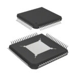 NB100EP223FAG

The activity of extra discounts on wholesale prices is in full swing…
Please fill in your contact information and we will send you the latest wholesale price list.






