 ChipApex | Global Electronic Components Supplier

SEARCH
Search Product
Search Post
— IC芯片 | 连接器 | 传感器 | 被动器件 —
Search productSearch post
— IC芯片 | 连接器 | 传感器 | 被动器件 —
Consult the customer manager about the wholesale price.
consultation hotline:86-132-6715-2157
email:[email protected]
Contact the product manager for consultation. One-stop consultation is available.
Do you want a lower wholesale price? Please send us your inquiry and we will reply immediately.
The NB2308AC1HD is a commercial-grade, 3.3 V zero delay clock buffer manufactured by onsemi. It features an integrated PLL that locks to an input clock on the REF pin, with feedback driven from one of eight outputs to the FBK pin. The device provides two banks of four buffered clock outputs each, controlled via select inputs S1 and S2. Key electrical parameters include an input frequency range of 15 MHz to 133 MHz, a supply voltage range of 3.0 V to 3.6 V, and an operating temperature range of 0°C to +70°C. Input-to-output propagation delay is guaranteed less than 250 ps, while output-to-output skew is less than 200 ps.
Verify package availability as the SOIC-16 variant may be subject to discontinuation or limited stock depending on the distributor. Confirm RoHS compliance status if lead-free packaging is required for assembly processes. Check current lifecycle status against project timelines to ensure long-term supply stability.
Select this part when a single-input, eight-output zero-delay buffer is required for commercial temperature ranges. Ensure the feedback path connects to an output with matching capacitive loading to achieve zero input-to-output delay. Verify that the 3.3 V supply voltage and 133 MHz maximum frequency meet system requirements.
This component belongs to the NB2308A family of zero delay buffers. The 'C' suffix indicates commercial temperature operation (0°C to +70°C), while 'H' denotes the high-drive version with faster rise and fall times compared to standard variants. It is functionally similar to other members like NB2308AI1HD but differs in temperature rating.
NB2308AI1HD: Industrial temperature grade (-40°C to +85°C). NB2308AC1D: Standard drive version (slower rise/fall times). NB2308AC1DTG: TSSOP-16 package alternative.
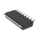 NB2308AC1HD

The activity of extra discounts on wholesale prices is in full swing…
Please fill in your contact information and we will send you the latest wholesale price list.






