 ChipApex | Global Electronic Components Supplier

SEARCH
Search Product
Search Post
— IC芯片 | 连接器 | 传感器 | 被动器件 —
Search productSearch post
— IC芯片 | 连接器 | 传感器 | 被动器件 —
Consult the customer manager about the wholesale price.
consultation hotline:86-132-6715-2157
email:[email protected]
Contact the product manager for consultation. One-stop consultation is available.
Do you want a lower wholesale price? Please send us your inquiry and we will reply immediately.
The NB2308AC3DG is a commercial-grade, 3.3 V zero delay clock buffer manufactured by onsemi in a 16-pin SOIC package. It features an internal PLL that locks to a reference input on the REF pin, with feedback driven from one of the outputs to the FBK pin. This configuration enables adjustable zero input-to-output propagation delay and low skew distribution. The device supports an input frequency range of 15 MHz to 133 MHz and provides eight buffered outputs organized into two banks of four. Each bank can be independently controlled via select inputs for tri-stating or bypass modes.
Verify the specific suffix 'DG' indicates a lead-free (Pb-Free) SOIC-16 package per the ordering information table. Confirm the operating temperature range corresponds to the 'C' suffix for Commercial grade (0°C to 70°C). Ensure the design utilizes the correct feedback path to achieve the intended 4X/2X multiplication ratios defined for the x3 configuration.
Select this component when a 4X or 2X clock multiplier is required alongside zero-delay buffering. The NB2308AC3DG specifically drives Bank A at 4X and Bank B at 2X (or Reference) depending on the feedback source. For applications requiring only 1X or 2X outputs, consider the NB2308AC1DG or NB2308AC2DG variants respectively. Ensure load capacitance requirements are met (15 pF for >100 MHz operation).
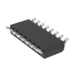 NB2308AC3DG

The activity of extra discounts on wholesale prices is in full swing…
Please fill in your contact information and we will send you the latest wholesale price list.





