 ChipApex | Global Electronic Components Supplier

SEARCH
Search Product
Search Post
— IC芯片 | 连接器 | 传感器 | 被动器件 —
Search productSearch post
— IC芯片 | 连接器 | 传感器 | 被动器件 —
Consult the customer manager about the wholesale price.
consultation hotline:86-132-6715-2157
email:[email protected]
Contact the product manager for consultation. One-stop consultation is available.
Do you want a lower wholesale price? Please send us your inquiry and we will reply immediately.
The NB2308AI1DG is a 3.3 V zero delay clock buffer manufactured by onsemi, designed for high-speed clock distribution in industrial applications. It features an internal phase-locked loop (PLL) that locks to a reference input on the REF pin, with feedback provided via the FBK pin. The device provides eight LVCMOS outputs organized into two banks of four, controlled by select inputs S1 and S2. It operates within a frequency range of 15 MHz to 133 MHz and supports supply voltages from 3.0 V to 3.6 V.
Verify the 'I' suffix indicates industrial temperature range (-40°C to +85°C). Confirm the 'DG' suffix denotes a lead-free SOIC-16 package. Check current availability status as this component may be subject to end-of-life notices or obsolescence.
Select NB2308AI1DG when a 1:8 ratio with reference frequency multiplication is required. Ensure output loading is balanced between the FBK pin and other outputs to maintain zero delay characteristics. Verify that the 15 pF load capacitance requirement at frequencies above 100 MHz fits the design constraints.
This part belongs to the NB2308A family of 3.3 V zero delay buffers. The 'I' suffix specifies the industrial operating temperature range, while 'C' would indicate commercial range. The 'G' suffix confirms Pb-Free packaging compliance.
Direct functional substitutes include other members of the NB2308A series such as NB2308AC1DG or NB2308AI1HDG, depending on drive strength and temperature requirements. Cross-vendor equivalents like IDT 2308 series parts may offer similar functionality but require verification of pinout and electrical parameters.
Zero delay is achieved by connecting one of the outputs to the FBK pin. To minimize delay variation, all outputs including the feedback source must have equal capacitive loading.
S1 and S2 are select inputs that control the state of the output banks. They can enable/disable specific banks or put the device into bypass mode where the REF input directly drives the outputs.
Yes. In the absence of an input clock, the device enters power-down mode, tri-stating the outputs and drawing less than 25 µA of current.
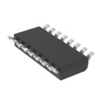 NB2308AI1DG

The activity of extra discounts on wholesale prices is in full swing…
Please fill in your contact information and we will send you the latest wholesale price list.






