 ChipApex | Global Electronic Components Supplier

SEARCH
Search Product
Search Post
— IC芯片 | 连接器 | 传感器 | 被动器件 —
Search productSearch post
— IC芯片 | 连接器 | 传感器 | 被动器件 —
Consult the customer manager about the wholesale price.
consultation hotline:86-132-6715-2157
email:[email protected]
Contact the product manager for consultation. One-stop consultation is available.
Do you want a lower wholesale price? Please send us your inquiry and we will reply immediately.
The NB2308AI3DTR2G is a 3.3 V zero delay clock buffer manufactured by onsemi, designed for distributing high-speed clocks. It features an internal PLL that locks to a reference clock input and allows feedback from any of its eight outputs. The device provides two banks of four buffered clock outputs each, with selectable three-state control via S1 and S2 inputs. It supports input frequencies from 15 MHz to 133 MHz and guarantees less than 250 ps input-to-output propagation delay and less than 200 ps output-to-output skew within the same bank.
Verify the industrial temperature range (-40°C to 85°C) and TSSOP-16 package configuration. Confirm the 'I' suffix indicates industrial grade and 'DT' indicates TSSOP packaging. Ensure compatibility with 3.3V supply requirements and check for lead-free (G suffix) availability if required by assembly specifications.
Select this part when 4x and 2x frequency multiplication is required simultaneously across separate output banks. Ensure equal loading on all outputs including the feedback pin to achieve zero input-output delay. Verify that the 15 pF load capacitance limit at frequencies above 100 MHz is met for optimal rise/fall times.
This component belongs to the NB2308A family of zero delay buffers. The '3' designation specifically configures the internal divider/multiplexer to provide 4x frequency on Bank A and 2x frequency on Bank B. Other variants like NB2308Ax1 provide reference frequency, while NB2308Ax4 provides 2x on all outputs.
NB2308AC3DTR2G offers the same functionality in commercial temperature range. NB2308AI3DR2G provides identical electrical characteristics but in SOIC-16 package instead of TSSOP-16.
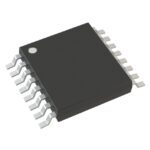 NB2308AI3DTR2G

The activity of extra discounts on wholesale prices is in full swing…
Please fill in your contact information and we will send you the latest wholesale price list.






