 ChipApex | Global Electronic Components Supplier

SEARCH
Search Product
Search Post
— IC芯片 | 连接器 | 传感器 | 被动器件 —
Search productSearch post
— IC芯片 | 连接器 | 传感器 | 被动器件 —
Consult the customer manager about the wholesale price.
consultation hotline:86-132-6715-2157
email:[email protected]
Contact the product manager for consultation. One-stop consultation is available.
Do you want a lower wholesale price? Please send us your inquiry and we will reply immediately.
The NB2308AI5HD is a 3.3 V zero delay clock buffer manufactured by onsemi, designed for high-speed clock distribution in industrial applications. It features an internal phase-locked loop (PLL) that locks to a reference input on the REF pin, with feedback driven from one of the outputs to the FBK pin. The device provides eight buffered clock outputs organized into two banks of four, controlled by select inputs S1 and S2. It supports input frequencies from 15 MHz to 133 MHz, guarantees input-to-output propagation delay under 250 ps, and output-to-output skew under 200 ps. The part operates within a supply voltage range of 3.0 V to 3.6 V and is housed in a 16-pin SOIC package.
Verify the specific suffix 'HD' indicates the high-drive variant with REF/2 configuration on both banks. Confirm the 'I' designation corresponds to the industrial temperature range (-40°C to +85°C). Ensure the 'D' suffix matches the required 16-pin SOIC package type rather than TSSOP. Check for lead-free availability if environmental compliance is required.
Select this component when low skew and zero input-output delay are critical for industrial environments. The high-drive version is suitable for heavier capacitive loads. Ensure the feedback path connects to an output that provides the desired frequency multiplication or division ratio according to the configuration table. Verify that the 3.3 V supply voltage aligns with the system design constraints.
This part belongs to the NB2308A family of zero delay buffers. The 'AI5H' designation specifies the industrial temperature grade, the fifth configuration variant (REF/2 on both banks), and the high-drive output strength. It is distinct from lower drive versions like NB2308AI1H and other configurations such as NB2308AI2 or NB2308AI4 which offer different frequency multiplication options.
NB2308AC5HD serves as the commercial temperature equivalent. NB2308AI5HDG is the lead-free version of the same device. Other family members like NB2308AI1HD or NB2308AI4D share the same package but differ in drive strength and frequency configuration.
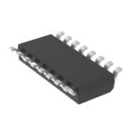 NB2308AI5HD

The activity of extra discounts on wholesale prices is in full swing…
Please fill in your contact information and we will send you the latest wholesale price list.





