 ChipApex | Global Electronic Components Supplier

SEARCH
Search Product
Search Post
— IC芯片 | 连接器 | 传感器 | 被动器件 —
Search productSearch post
— IC芯片 | 连接器 | 传感器 | 被动器件 —
Consult the customer manager about the wholesale price.
consultation hotline:86-132-6715-2157
email:[email protected]
Contact the product manager for consultation. One-stop consultation is available.
Do you want a lower wholesale price? Please send us your inquiry and we will reply immediately.
The NB2309AC1DTG is a 3.3 V zero delay clock buffer manufactured by onsemi, designed for distributing high-speed clocks in the 15 MHz to 133 MHz range. It accepts one reference input and drives nine low-skew outputs grouped as four plus four plus one. The device features an internal phase-locked loop (PLL) that locks to the REF pin input, with feedback obtained from the CLKOUT pad. It operates within a commercial temperature range of 0°C to 70°C and utilizes advanced 0.35 µm CMOS technology.
Verify the package suffix 'DT' corresponds to the TSSOP-16 form factor (CASE 948F). Confirm the 'C1' designation indicates the commercial temperature grade (0°C to 70°C) rather than industrial (-40°C to 85°C). Ensure the ordering code matches the specific shipping configuration required for production integration.
Select this component when a single reference clock must drive up to nine loads with minimal skew. The -1 variant provides standard drive strength; if faster rise and fall times are necessary, consider the -1H version. Ensure all outputs, including CLKOUT, have equal capacitive loading to maintain zero input-to-output delay characteristics.
This part belongs to the NB2309A family of 3.3 V zero delay buffers. Variants include the SOIC-16 package (suffix D), the TSSOP-16 package (suffix DT), and higher-drive -1H versions. The AC1DTR2G variant represents the same functional device in a tape-and-reel packaging format.
Public confirmed substitute part numbers: NB2309AI1DTG, NB2309AC1D, NB2309AC1DR2G.
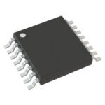 NB2309AC1DTG

The activity of extra discounts on wholesale prices is in full swing…
Please fill in your contact information and we will send you the latest wholesale price list.






