 ChipApex | Global Electronic Components Supplier

SEARCH
Search Product
Search Post
— IC芯片 | 连接器 | 传感器 | 被动器件 —
Search productSearch post
— IC芯片 | 连接器 | 传感器 | 被动器件 —
Consult the customer manager about the wholesale price.
consultation hotline:86-132-6715-2157
email:[email protected]
Contact the product manager for consultation. One-stop consultation is available.
Do you want a lower wholesale price? Please send us your inquiry and we will reply immediately.
NB3L8543SDTR2G is listed in the Clock Buffers, Drivers range at ChipApex. The manufacturer field lists onsemi. Its product description is IC CLK BUFFER 2:4 650MHZ 20TSSOP. Review the specifications below when checking this part for your BOM.
The NB3L8543SDTR2G is a high-performance, low-skew differential 2:1 multiplexer to 4 LVDS clock fanout buffer manufactured by onsemi. It features two selectable differential clock inputs (CLK/CLK and PCLK/PCLK) that support multiple logic families including LVPECL, LVDS, CML, HCSL, SSTL, and HSTL. The device provides four differential LVDS output pairs with a maximum operating frequency of 650 MHz at 3.3 V or 500 MHz at 2.5 V. Key electrical specifications include a typical additive phase jitter of 50 fs RMS, a maximum output skew of 40 ps, and a propagation delay of 1.9 ns. It operates within an ambient temperature range of -40°C to +85°C and is housed in a TSSOP-20 package.
Verify the ordering suffix 'R2G' corresponds to the Tape & Reel shipping configuration containing 2500 units per reel. Confirm the component is Pb-Free as indicated by the '/C0071' marking. Ensure the application design accounts for the specific thermal resistance values (140 °C/W junction-to-ambient at 0 lfpm) when calculating heat dissipation in enclosed environments.
Select this component when a single-ended or differential input must be routed to four LVDS loads with minimal skew. Choose between the CLK and PCLK inputs based on the source signal standard; PCLK supports CML while CLK does not. Ensure the power supply voltage matches the required maximum frequency, as the 650 MHz limit applies only at 3.3 V, whereas 2.5 V operation limits the frequency to 500 MHz.
This part belongs to the NB3L8543 family, which includes variants such as the NB3L8543E/D and NB3L8543S. The SDTR2G designation specifically identifies the surface-mount TSSOP-20 package version supplied in tape and reel format for automated assembly processes. It serves as a clock management solution within onsemi's portfolio of high-speed logic devices.
Direct functional substitutes within the same family include the NB3L8543SDTG, which shares identical electrical specifications but is shipped in rails rather than tape and reel. Cross-family replacements require verification of pin compatibility and electrical parameters against the original design requirements.
Explore related parts through Clock/Timing, Integrated Circuits (ICs), all product categories, ChipApex homepage.
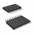 NB3L8543SDTR2G

The activity of extra discounts on wholesale prices is in full swing…
Please fill in your contact information and we will send you the latest wholesale price list.






