 ChipApex | Global Electronic Components Supplier

SEARCH
Search Product
Search Post
— IC芯片 | 连接器 | 传感器 | 被动器件 —
Search productSearch post
— IC芯片 | 连接器 | 传感器 | 被动器件 —
Consult the customer manager about the wholesale price.
consultation hotline:86-132-6715-2157
email:[email protected]
Contact the product manager for consultation. One-stop consultation is available.
Do you want a lower wholesale price? Please send us your inquiry and we will reply immediately.
NB3V1103CDTR2G is listed in the Clock Buffers, Drivers range at ChipApex. The manufacturer field lists onsemi. Its product description is IC CLK BUFFER 1:3 250MHZ 8TSSOP. Review the specifications below when checking this part for your BOM.
The NB3V1103CDTR2G is a 3.3 V LVCMOS low skew fanout buffer from the NB3V110xC series, manufactured by onsemi. It provides a 1:3 clock distribution with three outputs (Q0, Q1, Q2) in an 8-pin TSSOP package. The device supports asynchronous output enable control and operates within a supply voltage range of 3.0 V to 3.6 V at frequencies up to 250 MHz. Key electrical characteristics include a maximum propagation delay of 2.0 ns, output-to-output skew under 50 ps, and additive jitter below 200 fs. It functions across an extended temperature range of –40°C to +105°C.
Verify the ordering suffix 'DT' corresponds to the TSSOP-8 package and 'R2G' indicates tape and reel shipping configuration. Confirm RoHS compliance and lead-free status as specified in the datasheet attributes. Ensure the application environment stays within the recommended operating conditions for VDD and temperature to maintain specified performance metrics.
Select this component when a 1:3 fan-out ratio is required for LVCMOS signals. Compare against NB3V1102C (1:2) or NB3V1104C (1:4) if different output counts are needed, noting their pin compatibility. Consider the 250 MHz maximum frequency limit at 3.3 V operation. Verify that the required skew and jitter specifications align with the device's < 50 ps skew and < 200 fs jitter capabilities.
This part belongs to the NB3V110xC family of modular LVCMOS clock buffers. Family members including NB3V1102C, NB3V1104C, NB3V1106C, and NB3V1108C share similar high-performance characteristics and are designed for easy handling due to pin compatibility across variations.
NB3V1102CDTR2G offers 1:2 fan-out; NB3V1104CDTR2G offers 1:4 fan-out. Both are pin-compatible alternatives within the same family.
Explore related parts through Clock/Timing, Integrated Circuits (ICs), all product categories, ChipApex homepage.
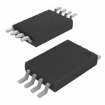 NB3V1103CDTR2G

The activity of extra discounts on wholesale prices is in full swing…
Please fill in your contact information and we will send you the latest wholesale price list.





