 ChipApex | Global Electronic Components Supplier

SEARCH
Search Product
Search Post
— IC芯片 | 连接器 | 传感器 | 被动器件 —
Search productSearch post
— IC芯片 | 连接器 | 传感器 | 被动器件 —
Consult the customer manager about the wholesale price.
consultation hotline:86-132-6715-2157
email:[email protected]
Contact the product manager for consultation. One-stop consultation is available.
Do you want a lower wholesale price? Please send us your inquiry and we will reply immediately.
NB4L16MMNR2 is listed in the Translators, Level Shifters range at ChipApex. The manufacturer field lists onsemi. Its product description is IC TRANSLTR UNIDIRECTIONAL 16QFN. Review the specifications below when checking this part for your BOM.
The NB4L16MMNR2 is a differential driver, receiver, buffer, and translator manufactured by onsemi. It accepts LVPECL, LVDS, CML, HSTL, LVCMOS, or LVTTL inputs and produces a 400 mV CML output. The device supports maximum input clock frequencies up to 3.5 GHz and data rates up to 5.0 Gb/s. It features internal 50 Ω termination resistors for both inputs and outputs, eliminating the need for external components. Operating within a VCC range of 2.375 V to 3.6 V with VEE at 0 V, it provides low jitter performance with typical propagation delay of 220 ps and rise/fall times of 60 ps. The component is housed in a 3x3 mm 16-pin QFN package.
Verify the specific ordering suffix against the manufacturer's current documentation to ensure correct packaging configuration. Confirm that the requested variant matches the required tape and reel specifications or tube quantities. Cross-reference the date code and assembly location markings with the latest datasheet revision to guarantee compliance with RoHS and halogen-free requirements. Ensure the supply voltage parameters align with the target application's power rails before finalizing procurement.
Select this component when interfacing between disparate logic families requiring translation to CML standards. The integrated termination resistors reduce bill-of-materials complexity compared to discrete solutions. Evaluate the operating temperature range and thermal resistance characteristics if the application involves high ambient temperatures or limited airflow. Consider the low jitter specifications for sensitive timing applications where signal integrity is critical.
This device belongs to the NB4L16M family of high-speed interface circuits designed for signal conditioning and level shifting. It functions as a versatile translator capable of handling various input formats while maintaining signal integrity through internal impedance matching. The family targets applications demanding high data throughput and low skew in compact form factors.
Consult official substitution guides for functionally compatible devices within the same product family. Verify pinout compatibility and electrical parameter equivalence before replacing existing components. Ensure any substitute part meets the same thermal and environmental ratings required by the original design.
For single-ended input configurations, connect the unused complementary differential input to the VBB pin, which serves as a switching reference voltage.
The VTD pins are used to connect the internal 50 Ω termination resistors to a common termination voltage, ensuring proper signal termination at the input stage.
Yes, for AC-coupled inputs, the VTD and VTD pins should be connected together and biased within the common mode range, typically using the VBB reference voltage.
Explore related parts through Logic, Integrated Circuits (ICs), all product categories, ChipApex homepage.
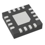 NB4L16MMNR2

The activity of extra discounts on wholesale prices is in full swing…
Please fill in your contact information and we will send you the latest wholesale price list.





