 ChipApex | Global Electronic Components Supplier
SEARCH
Search Product
Search Post
— IC芯片 | 连接器 | 传感器 | 被动器件 —
Search productSearch post
— IC芯片 | 连接器 | 传感器 | 被动器件 —
Consult the customer manager about the wholesale price.
consultation hotline:86-132-6715-2157
email:[email protected]
Contact the product manager for consultation. One-stop consultation is available.
Do you want a lower wholesale price? Please send us your inquiry and we will reply immediately.
The NB6L295MMNG is a dual-channel programmable clock and data delay line manufactured by onsemi. It features differential CML outputs and operates within a supply voltage range of 2.375 V to 3.6 V, supporting both 2.5 V and 3.3 V logic levels. The device provides two independent delay circuits housed in a QFN-24 package. Each channel offers 512 programmable taps with an increment of 11 ps, allowing for precise timing adjustments. The total available delay ranges from 3.2 ns to 8.5 ns for the first channel and 6.2 ns to 16.6 ns for the second. It functions reliably across an operating temperature range of -40°C to +85°C.
Verify component authenticity through authorized onsemi distributors or certified suppliers. Confirm RoHS compliance status via official documentation before integration. Check current lifecycle status as availability may vary. Ensure storage conditions meet moisture sensitivity level requirements to prevent damage during assembly processes.
Select this component when differential CML outputs are required for dual-channel delay applications. Compare against LVPECL variants if different output swing specifications are needed. Verify that the 512-tap resolution meets system timing accuracy requirements. Ensure the QFN-24 package footprint aligns with existing PCB layout constraints and thermal management strategies.
This part belongs to the NB6L295M series of programmable delay lines designed for high-performance timing applications. It serves as a specialized solution for managing skew in complex digital systems. The device complements other clock distribution components within the onsemi portfolio, offering flexible delay adjustment without external calibration.
The NB6L295MMNGEVB is an evaluation board for this device, not a direct functional substitute. For equivalent functionality, consider the NB6L295 (LVPECL output variant) if output compatibility allows. Verify pinout and electrical characteristics against alternative sources before implementation.


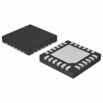 NB6L295MMNG
The activity of extra discounts on wholesale prices is in full swing…
Please fill in your contact information and we will send you the latest wholesale price list.




