 ChipApex | Global Electronic Components Supplier

SEARCH
Search Product
Search Post
— IC芯片 | 连接器 | 传感器 | 被动器件 —
Search productSearch post
— IC芯片 | 连接器 | 传感器 | 被动器件 —
Consult the customer manager about the wholesale price.
consultation hotline:86-132-6715-2157
email:[email protected]
Contact the product manager for consultation. One-stop consultation is available.
Do you want a lower wholesale price? Please send us your inquiry and we will reply immediately.
NB6N11SMNR2G is listed in the Clock Buffers, Drivers range at ChipApex. The manufacturer field lists onsemi. Its product description is IC CLK BUFFER 1:2 2GHZ 16QFN. Review the specifications below when checking this part for your BOM.
The NB6N11SMNR2G is a differential 1:2 clock or data receiver and translator from onsemi. It accepts AnyLevel input signals including LVPECL, CML, LVCMOS, LVTTL, and LVDS, translating them to LVDS outputs. The device operates up to 2.0 GHz for clocks or 2.5 Gb/s for data. It features a wide input common mode range from GND + 50 mV to VCC − 50 mV and includes internal 50 Ω termination resistors at the inputs. Packaged in a 3 mm x 3 mm QFN-16, it provides two identical LVDS output copies.
Verify the ordering suffix R2G corresponds to the tape and reel packaging configuration of 3000 units per reel. Confirm the component is Pb-Free and RoHS compliant as specified in the datasheet attributes. Ensure the QFN-16 package dimensions match the required PCB footprint layout for thermal management.
Select this component when a single high-speed differential or single-ended source must drive two LVDS destinations. It is suitable for designs requiring translation between various logic families and LVDS standards. Consider the 3.3 V supply requirement and the specific operating temperature range of -40°C to +85°C for environmental compatibility.
This part belongs to the ECLinPS MAX family of high-performance products by onsemi. It is functionally equivalent to legacy devices such as the EP11, LVEP11, SG11, and 7L11M. The NB6N11S series is designed for high-speed clock and data distribution in telecommunications and networking equipment.
Functionally compatible replacements include EP11, LVEP11, SG11, and 7L11M devices. Verify pinout and electrical specifications against these equivalents before substitution.
It supports AnyLevel inputs, including LVPECL, CML, LVCMOS, LVTTL, and LVDS.
The maximum input clock frequency is greater than 2.0 GHz.
The device provides two identical LVDS output pairs (Q0/Q0 and Q1/Q1).
Explore related parts through Clock/Timing, Integrated Circuits (ICs), all product categories, ChipApex homepage.
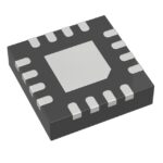 NB6N11SMNR2G

The activity of extra discounts on wholesale prices is in full swing…
Please fill in your contact information and we will send you the latest wholesale price list.




