 ChipApex | Global Electronic Components Supplier

SEARCH
Search Product
Search Post
— IC芯片 | 连接器 | 传感器 | 被动器件 —
Search productSearch post
— IC芯片 | 连接器 | 传感器 | 被动器件 —
Consult the customer manager about the wholesale price.
consultation hotline:86-132-6715-2157
email:[email protected]
Contact the product manager for consultation. One-stop consultation is available.
Do you want a lower wholesale price? Please send us your inquiry and we will reply immediately.
NB7VQ14MMNTXG is listed in the Clock Buffers, Drivers range at ChipApex. The manufacturer field lists onsemi. Its product description is IC CLK BUFFER 1:4 8.5GHZ 16QFN. Review the specifications below when checking this part for your BOM.
The NB7VQ14MMNTXG is a high-performance differential 1:4 CML fanout buffer from onsemi's GigaComm family. It operates with supply voltages of 1.8 V, 2.5 V, or 3.3 V and supports input clock frequencies up to 8.5 GHz and data rates up to 14 Gbps. The device features a selectable input equalizer to compensate for signal degradation in FR4 backplanes or cables. Key electrical parameters include a typical propagation delay of 165 ps, maximum output skew of 15 ps, and RMS clock jitter below 0.8 ps. It incorporates internal 50 Ω input termination resistors accessed via the VT pin, allowing compatibility with LVPECL, CML, and LVDS logic standards.
Verify the specific ordering suffix against the manufacturer's documentation to confirm packaging type. The NB7VQ14MMNTXG designation corresponds to the QFN-16 package. Confirm availability status as distribution channels may list varying stock levels or end-of-life statuses. Ensure the procurement source provides valid traceability for RoHS compliance and Pb-free certification as specified in the datasheet attributes.
Select this component when low output skew (<15 ps) and minimal jitter are critical for high-speed serial data integrity. The integrated equalizer is suitable for applications requiring signal regeneration across lossy interconnects like long FR4 traces. Ensure the design accommodates the required power supply range (1.71 V to 3.6 V) and thermal management for the QFN-16 package, specifically connecting the exposed pad to ground for heat dissipation.
This part belongs to the NB7VQ14M series within onsemi's GigaComm portfolio of high-performance clock products. It serves as a fanout buffer designed to drive multiple loads while maintaining signal quality. The MMNHTBG suffix indicates a tape and reel shipping configuration, distinct from tube packaging options available for other variants in the same functional family.
Direct replacements must match the 1:4 CML fanout topology, QFN-16 package, and comparable speed/jitter specifications. Verify that any substitute device supports the same multi-level input standards (LVPECL/CML/LVDS) and has compatible pinouts for the VT and EQEN control functions without requiring schematic modifications.
The equalizer is controlled by the EQEN pin. Setting EQEN Low bypasses the equalizer, while setting it High allows inputs to flow through the equalizer section. The default state at start-up is Low due to an internal pull-down resistor.
The NB7VQ14M accepts LVPECL, CML, and LVDS logic level standards. This is achieved through internal 50 Ω termination resistors accessed via the VT pin, which can be tied to appropriate voltage references or left open depending on the standard.
The device is rated for an ambient operating temperature range of -40°C to +85°C.
Explore related parts through Clock/Timing, Integrated Circuits (ICs), all product categories, ChipApex homepage.
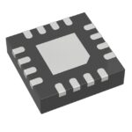 NB7VQ14MMNTXG

The activity of extra discounts on wholesale prices is in full swing…
Please fill in your contact information and we will send you the latest wholesale price list.





