 ChipApex | Global Electronic Components Supplier

SEARCH
Search Product
Search Post
— IC芯片 | 连接器 | 传感器 | 被动器件 —
Search productSearch post
— IC芯片 | 连接器 | 传感器 | 被动器件 —
Consult the customer manager about the wholesale price.
consultation hotline:86-132-6715-2157
email:[email protected]
Contact the product manager for consultation. One-stop consultation is available.
Do you want a lower wholesale price? Please send us your inquiry and we will reply immediately.
NBSG11BAHTBG is listed in the Clock Buffers, Drivers range at ChipApex. The manufacturer field lists onsemi. Its product description is IC CLK BUFFER 1:2 12GHZ 16FCBGA. Review the specifications below when checking this part for your BOM.
The NBSG11BAHTBG is a 2.5V/3.3V SiGe 1-to-2 differential fanout buffer manufactured by onsemi, designed for low skew and ultra-low jitter applications. It features internal 50Ω input termination resistors and accepts Negative ECL (NECL), Positive ECL (PECL), CML, LVCMOS, LVTTL, or LVDS inputs. The outputs are Reduced Swing ECL (RSECL) with a 400 mV peak-to-peak amplitude, typically loaded with 50Ω to VCC − 2 V. Operating at maximum clock frequencies up to 12 GHz typical, the device provides a propagation delay of 125 ps typical and rise/fall times of 30 ps typical.
Verify the specific ordering suffix HTBG against the manufacturer's current documentation to confirm package type and shipping configuration. Confirm that the component meets Pb-Free specifications as indicated in the datasheet attributes. Ensure compatibility with the intended operating voltage range of 2.375 V to 3.465 V for VCC.
Select this component when a 1-to-2 differential fanout buffer with ultra-low jitter is required. Ensure the design supports the specified supply voltages and termination requirements. Verify that the QFN16 package dimensions and thermal characteristics align with the PCB layout constraints.
The NBSG11BAHTBG belongs to the NBSG11 family of high-speed SiGe differential clock drivers. This series is optimized for applications demanding precise timing and minimal signal distortion. The device integrates internal termination to simplify circuit design and reduce external component count.
Consult the manufacturer's official replacement guide for verified substitutes. Ensure any alternative component matches the pinout, electrical characteristics, and package dimensions of the NBSG11BAHTBG.
The NBSG11 accepts Negative ECL (NECL), Positive ECL (PECL), CML, LVCMOS, LVTTL, and LVDS input signals.
The typical propagation delay is 125 ps across the operating temperature range.
Outputs are typically terminated with 50Ω resistors to VTT = VCC − 2.0 V.
Explore related parts through Clock/Timing, Integrated Circuits (ICs), all product categories, ChipApex homepage.
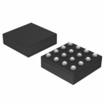 NBSG11BAHTBG

The activity of extra discounts on wholesale prices is in full swing…
Please fill in your contact information and we will send you the latest wholesale price list.






