 ChipApex | Global Electronic Components Supplier

SEARCH
Search Product
Search Post
— IC芯片 | 连接器 | 传感器 | 被动器件 —
Search productSearch post
— IC芯片 | 连接器 | 传感器 | 被动器件 —
Consult the customer manager about the wholesale price.
consultation hotline:86-132-6715-2157
email:[email protected]
Contact the product manager for consultation. One-stop consultation is available.
Do you want a lower wholesale price? Please send us your inquiry and we will reply immediately.
NBSG11MNR2G is listed in the Clock Buffers, Drivers range at ChipApex. The manufacturer field lists onsemi. Its product description is NBSG11 - BBG 1:2 DIFF CLOCK DRIV. Review the specifications below when checking this part for your BOM.
The NBSG11MNR2G is a 1-to-2 differential fanout buffer manufactured by onsemi, designed for low skew and ultra-low jitter applications. It accepts inputs from Negative ECL (NECL), Positive ECL (PECL), CML, LVCMOS, LVTTL, or LVDS signals. The device features Reduced Swing ECL (RSECL) outputs with a 400 mV peak-to-peak amplitude. It incorporates internal 50 Ω termination resistors at the input pins. The maximum input clock frequency reaches 12 GHz typical, with a propagation delay of 125 ps typical. It operates within a supply voltage range of 2.375 V to 3.465 V for VCC or -2.375 V to -3.465 V for VEE, housed in a QFN-16 package.
Verify the specific ordering suffix 'MN' corresponds to the QFN-16 package and tape & reel shipping configuration as defined in the manufacturer's documentation. Confirm that the thermal exposed pad requirements are met during PCB assembly to ensure proper heat dissipation and electrical connection to VEE if required by the design.
Select this component when a differential fanout buffer with high-frequency capability up to 12 GHz is required. Ensure the system power supply aligns with the specified RSPECL or RSNECL operating ranges. Consider the internal 50 Ω termination when designing input matching networks to avoid additional discrete components.
This part belongs to the NBSG11 series of SiGe differential clock drivers. It is specifically engineered for applications demanding precise timing and signal integrity. The device provides both inverted and non-inverted outputs to facilitate flexible routing in complex circuit layouts.
Publicly confirmed substitute part numbers are not available in the provided documentation. Evaluate alternative devices based on pin compatibility, electrical specifications, and package dimensions before implementation.
The NBSG11 supports Negative ECL (NECL), Positive ECL (PECL), Current Mode Logic (CML), Low Voltage CMOS (LVCMOS), Low Voltage TTL (LVTTL), and Low Voltage Differential Signaling (LVDS).
The device includes internal 50 Ω termination resistors connected to the VTCLK and VTCLK pins. These can be utilized directly or connected to appropriate supply voltages depending on the input format.
The typical propagation delay is 125 ps, with a guaranteed range between 90 ps and 160 ps across the operating temperature range.
Explore related parts through Clock/Timing, Integrated Circuits (ICs), all product categories, ChipApex homepage.
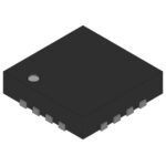 NBSG11MNR2G

The activity of extra discounts on wholesale prices is in full swing…
Please fill in your contact information and we will send you the latest wholesale price list.





