 ChipApex | Global Electronic Components Supplier

SEARCH
Search Product
Search Post
— IC芯片 | 连接器 | 传感器 | 被动器件 —
Search productSearch post
— IC芯片 | 连接器 | 传感器 | 被动器件 —
Consult the customer manager about the wholesale price.
consultation hotline:86-132-6715-2157
email:[email protected]
Contact the product manager for consultation. One-stop consultation is available.
Do you want a lower wholesale price? Please send us your inquiry and we will reply immediately.
NBSG16MNG is listed in the Specialty Logic range at ChipApex. The manufacturer field lists onsemi. Its product description is IC TRANSCEIVER 16QFN. Review the specifications below when checking this part for your BOM.
The NBSG16MNG is a differential receiver/driver utilizing SiGe technology, designed for high-frequency applications. It features RSECL outputs with a 400 mV peak-to-peak swing and incorporates internal 50 Ω input termination resistors. The device supports multiple input standards including NECL, PECL, HSTL, LVTTL, LVCMOS, CML, and LVDS. It operates within a supply voltage range of 2.375 V to 3.465 V (VCC) or -2.375 V to -3.465 V (VEE). Key electrical characteristics include a maximum typical input clock frequency exceeding 12 GHz, a typical propagation delay of 120 ps, and rise/fall times of 40 ps.
Verify the specific suffix 'MN' corresponds to the QFN-16 package configuration before ordering. Confirm that the required operating temperature range aligns with the specified -40°C to +85°C limits. Ensure power supply decoupling capacitors are placed close to the VBB and VMM pins if utilized. Check for any applicable export control classifications such as ECCN 3A001A11B.
Select this component when interfacing between different logic families requiring level translation without external resistors. The internal termination reduces board space and improves signal integrity at frequencies above 10 GHz. Consider the thermal resistance requirements of the QFN-16 package for adequate heat dissipation in dense layouts.
This device belongs to the NBSG16 family of SiGe differential receivers/drivers. It serves as a functional equivalent to older EP16 and LVEP16 devices but offers higher bandwidth and lower electromagnetic interference capabilities. The family includes variants like NBSG16BA and NBSG16MNR2G, differing primarily in packaging and shipping quantities.
Public confirmed substitute part numbers: EP16, LVEP16.
Unused complementary differential inputs must be connected to either the VBB or VMM pin to serve as a switching reference voltage for single-ended input conditions.
The VTD pins connect to internal 50 Ω termination resistors. For CML interfaces, they should be connected to VCC; for LVDS, they should be connected together.
Explore related parts through Logic, Integrated Circuits (ICs), all product categories, ChipApex homepage.
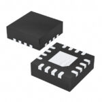 NBSG16MNG

The activity of extra discounts on wholesale prices is in full swing…
Please fill in your contact information and we will send you the latest wholesale price list.






