 ChipApex | Global Electronic Components Supplier

SEARCH
Search Product
Search Post
— IC芯片 | 连接器 | 传感器 | 被动器件 —
Search productSearch post
— IC芯片 | 连接器 | 传感器 | 被动器件 —
Consult the customer manager about the wholesale price.
consultation hotline:86-132-6715-2157
email:[email protected]
Contact the product manager for consultation. One-stop consultation is available.
Do you want a lower wholesale price? Please send us your inquiry and we will reply immediately.
NBSG16VSMNHTBG is listed in the Specialty Logic range at ChipApex. The manufacturer field lists onsemi. Its product description is IC TRANSCEIVER 16QFN. Review the specifications below when checking this part for your BOM.
The NBSG16VSMNHTBG is a high-frequency differential receiver/driver manufactured by onsemi in a QFN-16 package. It operates with variable output swing, supporting PECL and NECL configurations across supply voltages of 2.375 V to 3.465 V. The device features internal 50 Ω input termination resistors and accepts inputs from NECL, PECL, LVTTL, LVCMOS, CML, or LVDS standards. It achieves a maximum typical input clock frequency of 12 GHz and data rates up to 12 Gb/s, with typical rise/fall times of 40 ps and propagation delay of 120 ps.
Verify the specific suffix HTBG indicates the QFN-16 package configuration and tape-and-reel shipping format containing 100 units per reel. Confirm Pb-free status and ensure compatibility with the required operating temperature range of -40°C to +85°C before finalizing procurement specifications.
Select this component when variable output amplitude control is required for high-speed differential signaling. Ensure the design supports the necessary supply voltage ranges and utilizes the internal termination resistors to minimize external components. Verify that the interface standards match the supported input types such as PECL or NECL.
This part belongs to the NBSG16VS family of SiGe differential receiver/drivers. It serves as a functional equivalent to the EP16VS device but offers higher bandwidth and lower electromagnetic interference capabilities. The product line targets applications demanding precise signal integrity and adjustable output levels in high-frequency environments.
The datasheet does not list confirmed substitute part numbers for the NBSG16VSMNHTBG. Designers should evaluate the NBSG16VSBAHTBG (FCBGA-16 package) if package form factor changes are permissible, though electrical characteristics remain consistent within the family.
The output amplitude is varied by applying a control voltage to the VCTRL input pin, allowing adjustment between 100 mV and 750 mV peak-to-peak.
VBB provides a reference voltage for single-ended NECL or PECL inputs, while VMM serves as a reference for LVCMOS inputs. They can also be used to rebias AC-coupled inputs.
Explore related parts through Logic, Integrated Circuits (ICs), all product categories, ChipApex homepage.
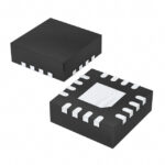 NBSG16VSMNHTBG

The activity of extra discounts on wholesale prices is in full swing…
Please fill in your contact information and we will send you the latest wholesale price list.






