 ChipApex | Global Electronic Components Supplier

SEARCH
Search Product
Search Post
— IC芯片 | 连接器 | 传感器 | 被动器件 —
Search productSearch post
— IC芯片 | 连接器 | 传感器 | 被动器件 —
Consult the customer manager about the wholesale price.
consultation hotline:86-132-6715-2157
email:[email protected]
Contact the product manager for consultation. One-stop consultation is available.
Do you want a lower wholesale price? Please send us your inquiry and we will reply immediately.
NBXDBB018LN1TAG is listed in the Programmable Timers And Oscillators range at ChipApex. The manufacturer field lists onsemi. Its product description is IC OSC XTAL DUAL FREQ 6-CLCC. Review the specifications below when checking this part for your BOM.
The NBXDBB018LN1TAG is a dual-frequency crystal oscillator from the PureEdge family, designed for 3.3 V LVPECL clock generation. It provides selectable outputs of 155.52 MHz or 311.04 MHz using a high Q fundamental crystal and PLL multiplier. The device features ultra-low jitter (0.4 ps RMS) and phase noise. It operates within a commercial temperature range (-40°C to +85°C) with a total frequency stability of ±20 PPM. Packaged in a hermetically sealed 6-pin CLCC SMD case, it supports networking and SONET/SDH applications.
Verify the specific ordering suffix 'LN1TAG' corresponds to the 1000-unit tape and reel packaging configuration. Confirm that the 'B' designation in the base part number aligns with the required ±20 PPM frequency stability for commercial temperature ranges rather than the industrial variant.
Select this component when a 3.3 V supply and LVPECL interface are required for low-jitter clocking. Ensure the design accommodates the 170 kΩ internal pull-up resistors on the OE and FSEL pins, which default to active and 155.52 MHz respectively if left floating.
This part belongs to the NBXDBB/NBXDBA series of dual-frequency oscillators. The 'B' suffix indicates ±20 PPM stability for commercial temperatures, while 'A' denotes ±50 PPM for industrial ranges. It shares the same physical footprint and electrical interface as the NBXDBA018LN1TAG.
The NBXDBA018LN1TAG serves as a direct functional substitute with identical pinout and performance, differing only in frequency stability specifications (±50 PPM vs. ±20 PPM).
The default output frequency is 155.52 MHz, which occurs when the FSEL pin is left open or driven HIGH.
The output is active by default because the OE pin has an internal 170 kΩ pull-up resistor. Driving the OE pin LOW places the outputs in a high-impedance state.
Outputs should be terminated with 50 Ω receiver termination resistors connected to VTT = VDD - 2.0 V.
Explore related parts through Clock/Timing, Integrated Circuits (ICs), all product categories, ChipApex homepage.
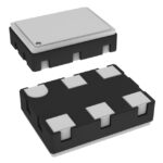 NBXDBB018LN1TAG

The activity of extra discounts on wholesale prices is in full swing…
Please fill in your contact information and we will send you the latest wholesale price list.





