 ChipApex | Global Electronic Components Supplier
SEARCH
Search Product
Search Post
— IC芯片 | 连接器 | 传感器 | 被动器件 —
Search productSearch post
— IC芯片 | 连接器 | 传感器 | 被动器件 —
Consult the customer manager about the wholesale price.
consultation hotline:86-132-6715-2157
email:[email protected]
Contact the product manager for consultation. One-stop consultation is available.
Do you want a lower wholesale price? Please send us your inquiry and we will reply immediately.
The NBXSGA008LN1TAG is a single-frequency crystal oscillator (XO) from onsemi’s PureEdge/C0116 family, designed for 2.5 V or 3.3 V LVPECL clock generation applications. It utilizes a high-Q fundamental mode crystal and a Phase Lock Loop (PLL) multiplier to deliver an output frequency of 161.1328 MHz with ultra-low jitter and phase noise. The device features hermetically sealed ceramic SMD packaging in a 6-pin CLCC format. Key electrical specifications include a typical RMS phase jitter of 0.5 ps between 12 kHz and 20 MHz, a power supply current of approximately 91 mA at 2.5 V, and total frequency stability of ±50 ppm.
Verify the specific ordering suffix against the manufacturer's Tape and Reel Packaging Specification Brochure (BRD8011/D) to confirm part orientation and tape dimensions. Confirm that the required quantity matches the available reel sizes of 100 or 1,000 units. Ensure compatibility with the specified operating voltage range of 2.5 V ±5% or 3.3 V ±10% before procurement.
Select this component when a precise 161.1328 MHz LVPECL clock signal is required for high-speed networking or storage interfaces. The device supports both 2.5 V and 3.3 V logic levels, offering flexibility in system design. Consider the hermetically sealed ceramic package if environmental robustness against shock, vibration, and thermal stress is necessary for the application environment.
This oscillator belongs to the PureEdge/C0116 clock family, which provides accurate and precision clock solutions. It is functionally similar to other devices in the NBXSGA series, such as the NBXSGA008LNHTAG, which shares the same core oscillator specifications but differs in shipping quantity per reel.
The NBXSGA008LNHTAG serves as a direct functional substitute with identical electrical characteristics, differing only in the shipping quantity (100 units per reel versus 1,000 units). Verify package compatibility and ensure the replacement meets the same MIL-STD-833 mechanical reliability standards.
The OE pin accepts LVTTL/LVCMOS control signals. When left floating, it defaults to a logic HIGH state, keeping the output active. A LOW level input places the output pins in a High-Z state.
The CLK and CLK_n outputs should typically be loaded with 50 Ω receiver termination resistors connected to VTT, where VTT equals VDD minus 2.0 V.
The maximum rating for the positive power supply (VDD) is 4.6 V when GND is at 0 V. Exceeding this stress rating may damage the device.



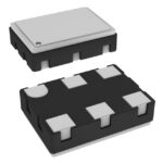 NBXSGA008LN1TAG
The activity of extra discounts on wholesale prices is in full swing…
Please fill in your contact information and we will send you the latest wholesale price list.



