 ChipApex | Global Electronic Components Supplier

SEARCH
Search Product
Search Post
— IC芯片 | 连接器 | 传感器 | 被动器件 —
Search productSearch post
— IC芯片 | 连接器 | 传感器 | 被动器件 —
Consult the customer manager about the wholesale price.
consultation hotline:86-132-6715-2157
email:[email protected]
Contact the product manager for consultation. One-stop consultation is available.
Do you want a lower wholesale price? Please send us your inquiry and we will reply immediately.
The NC7SZ32L6X-L22175 is a single two-input OR gate from onsemi’s TinyLogic UHS series, fabricated with advanced CMOS technology. It operates within a broad VCC range of 1.65 V to 5.5 V and features high output drive capability of ±24 mA at 3 V. The device provides ultra-high speed performance with a typical propagation delay of 2.4 ns into 50 pF at 5 V. Inputs tolerate voltages up to 5.5 V independent of the operating voltage, facilitating 5 V to 3 V translation. It includes power-down high-impedance inputs/outputs and proprietary noise/EMI reduction circuitry.
Verify component authenticity through authorized distributors or direct manufacturer channels. Confirm RoHS compliance and Pb-free status as specified in the datasheet. Check for discontinuation notices regarding specific lot codes or ordering suffixes. Ensure storage conditions adhere to recommended temperature ranges to maintain reliability. Validate package markings against official documentation to prevent counterfeit substitution.
Select this component for designs requiring a single OR gate with minimal footprint and high switching speeds. Consider the MicroPak package for space-constrained PCB layouts. Evaluate the 1.65 V to 5.5 V operating range against system supply rails. Assess input tolerance requirements if interfacing with 5 V logic levels while operating at lower voltages. Review thermal resistance values for adequate heat dissipation in enclosed environments.
This part belongs to the TinyLogic UHS family, designed for ultra-high speed digital logic applications. It complements other single-function gates within the NC7SZ series, offering comparable performance to LCX devices at 3.3 V. The MicroPak package provides a compact solution for modern surface-mount assembly processes. It serves as a drop-in replacement for legacy logic families in portable and battery-operated devices.
NC7SZ32M5X-L22090 (SOT23-5)
The inputs are tolerant up to 5.5 V regardless of the VCC operating voltage, allowing safe interface with 5 V logic signals even when the device operates at lower voltages like 3.3 V.
When VCC is 0 V, both the inputs and outputs enter a high-impedance state, effectively preventing current flow and reducing power consumption in standby modes.
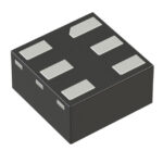 NC7SZ32L6X-L22175

The activity of extra discounts on wholesale prices is in full swing…
Please fill in your contact information and we will send you the latest wholesale price list.




