 ChipApex | Global Electronic Components Supplier
NCP51400MNTXG
Search Product
Search Post
— IC芯片 | 连接器 | 传感器 | 被动器件 —
Search productSearch post
— IC芯片 | 连接器 | 传感器 | 被动器件 —
Consult the customer manager about the wholesale price.
consultation hotline:86-132-6715-2157
email:[email protected]
Contact the product manager for consultation. One-stop consultation is available.
Do you want a lower wholesale price? Please send us your inquiry and we will reply immediately.
The NCP51400MNTXG is a DDR termination regulator designed for low input voltage and low noise systems. It integrates a high-performance LDO linear regulator capable of simultaneous source and sink current delivery. The device supports input voltages from 2.375 V to 5.5 V, with an output voltage range up to 750 mV. It features a fast feedback loop allowing the use of small ceramic capacitors for rapid load transient response, requiring a minimum of 20 μF output capacitance. The part operates within a temperature range of -40°C to +125°C and draws 700 μA of input current.
Verify the specific ordering suffix against the manufacturer's official documentation to ensure correct packaging and tape specifications. Confirm that the component meets RoHS compliance requirements for your target assembly process. Cross-reference the datasheet revision date to ensure all electrical characteristics and pin configurations align with your design specifications before finalizing procurement.
Select this component when designing systems requiring precise tracking termination for various DDR memory generations. Ensure the input voltage rail falls within the 2.375 V to 5.5 V range and that the required output current does not exceed 3 A. Consider the DFN-10 package size for space-constrained layouts and verify that the remote sense capability can be effectively utilized to maintain accuracy across PCB traces.
This device belongs to the NCP51400 series of specialized power management ICs focused on DDR termination applications. It is part of Onsemi's portfolio aimed at reducing component count and board space in memory subsystems. The series provides integrated solutions that replace discrete resistor networks and separate regulators, simplifying the design of high-speed memory interfaces.
Publicly confirmed substitute part numbers are not available in the provided documentation. Designers should consult the manufacturer's official replacement guide or contact technical support directly for validated cross-reference information. Do not assume functional compatibility with other DDR termination regulators without verifying pinouts and electrical parameters.
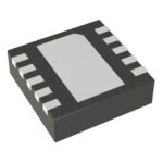 NCP51400MNTXG
The activity of extra discounts on wholesale prices is in full swing…
Please fill in your contact information and we will send you the latest wholesale price list.





