 ChipApex | Global Electronic Components Supplier
NCP51401MNTXG
Search Product
Search Post
— IC芯片 | 连接器 | 传感器 | 被动器件 —
Search productSearch post
— IC芯片 | 连接器 | 传感器 | 被动器件 —
Consult the customer manager about the wholesale price.
consultation hotline:86-132-6715-2157
email:[email protected]
Contact the product manager for consultation. One-stop consultation is available.
Do you want a lower wholesale price? Please send us your inquiry and we will reply immediately.
The NCP51401MNTXG is a source/sink dual data rate (DDR) termination regulator designed for low input voltage, low noise, and space-constrained systems. It features integrated power MOSFETs to minimize external component count. The device supports an input voltage range of 2.375 V to 5.5 V and delivers up to 3 A output current. It maintains fast transient response with a minimum output capacitance of 20 μF. Operating temperatures range from -40°C to +125°C.
Verify the complete part number including suffixes such as 'MNTXG' against official onsemi documentation to ensure correct packaging and tape specifications. Confirm RoHS compliance status through the manufacturer's latest environmental reports. Cross-reference the datasheet revision date to validate technical parameters before integration into design files.
Select this component when designing systems requiring precise DDR termination with minimal output capacitance requirements. The integrated MOSFET architecture suits applications where PCB area is limited. Ensure the input voltage rail falls within the specified operational range. Consider the thermal performance characteristics relative to the expected load current and ambient operating conditions.
This device belongs to the NCP5140x series of specialized power management ICs focused on memory termination. It complements other regulators in the portfolio by addressing specific DDR interface requirements. The series targets modern computing platforms demanding high efficiency and compact form factors for memory subsystem power delivery.
Public confirmed substitute part numbers are not available in the provided documentation.
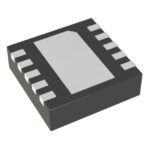 NCP51401MNTXG
The activity of extra discounts on wholesale prices is in full swing…
Please fill in your contact information and we will send you the latest wholesale price list.





