 ChipApex | Global Electronic Components Supplier
NCP51403MNTXG
Search Product
Search Post
— IC芯片 | 连接器 | 传感器 | 被动器件 —
Search productSearch post
— IC芯片 | 连接器 | 传感器 | 被动器件 —
Consult the customer manager about the wholesale price.
consultation hotline:86-132-6715-2157
email:[email protected]
Contact the product manager for consultation. One-stop consultation is available.
Do you want a lower wholesale price? Please send us your inquiry and we will reply immediately.
The NCP51403MNTXG is a specialized DDR termination regulator from onsemi, designed for high-speed memory applications. It provides a 3 A output current capability with an input voltage range of 2.375 V to 5.5 V and a maximum output voltage of 750 mV. The device operates within a temperature range of -40 °C to +125 °C and draws an operating supply current of 700 uA. Packaged in a 10-pin DFN surface-mount format, it supports DDR1, DDR2, DDR3, LPDDR3, and DDR4 standards without droop.
Verify the specific package marking and date code against the manufacturer's latest datasheet to ensure authenticity. Confirm that the 10-pin DFN footprint matches the design layout requirements. Check for any recent product change notifications regarding packaging materials or manufacturing site changes. Ensure compatibility with the target DDR standard's electrical specifications before finalizing procurement.
Select this component when designing systems requiring dedicated VTT termination for DDR memory buses. It is suitable for applications needing a 3 A source/sink capability with tight voltage regulation. Consider the 10-pin DFN package for space-constrained designs. Verify that the input voltage range aligns with the system's available power rails and that the thermal performance meets the operating environment requirements.
This part belongs to the NCP51400 series of DDR termination regulators from onsemi. It shares functional similarities with other members like the NCP51400 and NCP51401 but is specifically characterized for broader DDR compatibility. The series is designed to replace discrete resistor networks, offering better accuracy and lower board space usage in high-speed digital systems.
Direct substitutes include NCP51400MNTXG and NCP51401MNTXG from the same family. Verify pinout compatibility and specific electrical tolerances before substitution. Other DDR termination regulators from different manufacturers may require schematic and layout modifications.
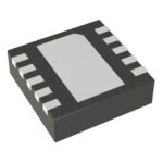 NCP51403MNTXG
The activity of extra discounts on wholesale prices is in full swing…
Please fill in your contact information and we will send you the latest wholesale price list.







