 ChipApex | Global Electronic Components Supplier

SEARCH
Search Product
Search Post
— IC芯片 | 连接器 | 传感器 | 被动器件 —
Search productSearch post
— IC芯片 | 连接器 | 传感器 | 被动器件 —
Consult the customer manager about the wholesale price.
consultation hotline:86-132-6715-2157
email:[email protected]
Contact the product manager for consultation. One-stop consultation is available.
Do you want a lower wholesale price? Please send us your inquiry and we will reply immediately.
NCP752BSN18T1G is listed in the Voltage Regulators - Linear, Low Drop Out (LDO) Regulators range at ChipApex. The manufacturer field lists onsemi. Its product description is IC REG LINEAR 1.8V 200MA 5-TSOP. Review the specifications below when checking this part for your BOM.
The NCP752BSN18T1G is a fixed-output low dropout regulator providing 1.8 V at up to 200 mA. It features ultra-low quiescent current of 12 µA and ultra-low noise of 11.5 µVRMS from 100 Hz to 100 kHz. The device operates with an input voltage range of 2.0 V to 5.5 V, offering high power supply rejection ratio of 68 dB at 1 kHz. It includes an enable pin, open-drain power good output, internal soft-start, thermal shutdown, and active output discharge.
Verify the specific suffix 'B' indicates the Power Good timeout delay characteristics defined in the datasheet electrical specifications. Confirm the package type matches the required PCB footprint, as the NCP752 series is available in TSOP-5 and XDFN packages. Ensure the ordering part number aligns with the desired fixed output voltage option within the 0.8 V to 3.5 V range.
Select this component when ultra-low noise and low quiescent current are critical for portable or RF designs. The NCP752BSN18T1G provides a stable 1.8 V output with minimal external component requirements. Consider the enable pin functionality for power management and the power good output for system status monitoring. Verify that the load transient response meets the application's dynamic requirements.
The NCP752 series is designed by onsemi as a high-performance LDO for noise-sensitive applications. It combines low dropout voltage with excellent line and load regulation. The device is optimized for portable electronics where battery life and signal integrity are paramount. The NCP752BSN18T1G represents a specific variant with fixed 1.8 V output and B-series timing characteristics.
Check for direct substitutes within the NCP752 family with different output voltages or package options. Verify compatibility with existing PCB layouts if switching between TSOP-5 and XDFN packages. Ensure replacement parts maintain similar noise and PSRR specifications for RF applications.
The typical quiescent current is 12 µA at no-load conditions.
Yes, a minimum of 1.0 µF ceramic capacitor is recommended on both the input and output pins for stability.
The Power Good output is an open-drain pin that indicates when the output voltage has reached its regulated level.
Explore related parts through Power Management (PMIC), Integrated Circuits (ICs), all product categories, ChipApex homepage.
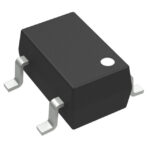 NCP752BSN18T1G

The activity of extra discounts on wholesale prices is in full swing…
Please fill in your contact information and we will send you the latest wholesale price list.




