 ChipApex | Global Electronic Components Supplier
NCP81152MNTWG
Search Product
Search Post
— IC芯片 | 连接器 | 传感器 | 被动器件 —
Search productSearch post
— IC芯片 | 连接器 | 传感器 | 被动器件 —
Consult the customer manager about the wholesale price.
consultation hotline:86-132-6715-2157
email:[email protected]
Contact the product manager for consultation. One-stop consultation is available.
Do you want a lower wholesale price? Please send us your inquiry and we will reply immediately.
The NCP81152MNTWG is a synchronous buck dual MOSFET gate driver manufactured by onsemi. It operates within an input voltage range of 4.5 V to 5.5 V and supports an operating temperature range from -40°C to +100°C. The device utilizes a 16-VFQFN exposed pad package with dimensions of 2.5x3.5 mm. Key electrical characteristics include a maximum high-side turn-on delay of 15 ns, low-side turn-on delay of 8 ns, high-side turn-off delay of 18 ns, and low-side turn-off delay of 15 ns. Rise and fall times are specified at 16 ns and 11 ns respectively.
Verify the specific suffix MNTWG against the official datasheet to confirm the 16-QFN package and industrial temperature rating. Ensure compatibility with the required PWM logic levels and bootstrap capacitor requirements. Confirm RoHS compliance status through the manufacturer's current documentation before finalizing procurement specifications.
Select this component for applications requiring a dedicated dual MOSFET driver optimized for synchronous buck topologies. The integrated zero-cross detection and adaptive anti-cross-conduction features make it suitable for high-efficiency designs where minimizing switching losses is critical. Verify that the 4.5 V to 5.5 V supply range aligns with the system's available bias voltage.
This part belongs to the NCP8115x series of specialized PMICs designed for power management. It functions as a high-side and low-side gate driver pair, distinct from single-channel drivers or full-bridge configurations. The device integrates control logic directly with the driver stage to simplify schematic design for synchronous rectification applications.
Consult official substitution guides for verified equivalents. Generic cross-references may not match the specific timing parameters or zero-cross detection features. Verify pinout compatibility and thermal performance if considering alternative packages.
It precisely controls the conduction of high-side and low-side FETs, allowing the converter to operate in diode emulation mode during light loads, thereby reducing switching losses.
The FLAG pin serves as a thermal flag output. It indicates when the junction temperature exceeds a safe threshold, though it has no direct electrical connection to the internal circuitry other than the thermal sensing mechanism.
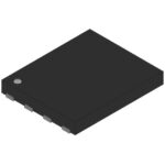 NCP81152MNTWG
The activity of extra discounts on wholesale prices is in full swing…
Please fill in your contact information and we will send you the latest wholesale price list.





