ChipApex | Global Electronic Components Supplier
NCV51313AMNWTWG
Search Product
Search Post
— IC芯片 | 连接器 | 传感器 | 被动器件 —
Search productSearch post
— IC芯片 | 连接器 | 传感器 | 被动器件 —
Consult the customer manager about the wholesale price.
consultation hotline:86-132-6715-2157
email:[email protected]
Contact the product manager for consultation. One-stop consultation is available.
Do you want a lower wholesale price? Please send us your inquiry and we will reply immediately.
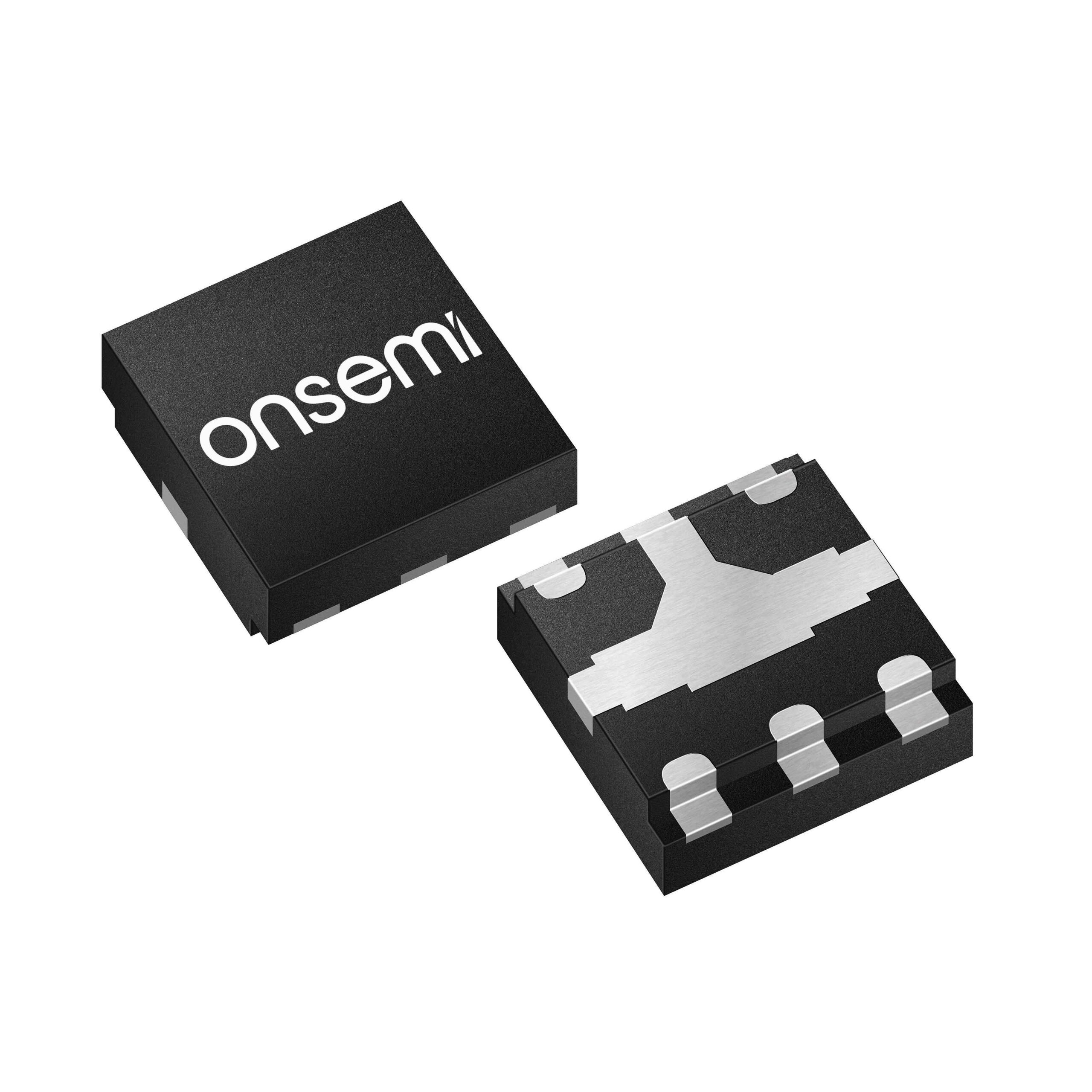
The NCV51313AMNWTWG is an automotive-grade high-side gate driver from onsemi, designed for DC-DC converters and inverters. It features a supply voltage range of 8 V to 19 V and supports CMOS/TTL logic inputs. The device provides a 2.0 A source current and a 3.0 A sink current capability. Key electrical parameters include a typical rise time of 11 ns and a fall time of 10 ns. Maximum delay times are specified at 100 ns for both turn-on and turn-off states. It operates within a junction temperature range of -40 °C to +125 °C and utilizes a DFNW-6 surface-mount package.
Verify the specific suffix 'TWG' against the manufacturer's official documentation to confirm RoHS compliance and lead-free status. Ensure the ordering part number matches the exact package variant required for your PCB layout. Confirm that the component meets the necessary automotive qualification standards for your intended application environment before finalizing procurement.
Select this component when designing high-frequency power circuits requiring precise timing control. The NCV51313A variant offers a typical propagation delay of 50 ns, suitable for general-purpose switching applications. Consider the DFNW-6 package for space-constrained designs due to its compact 3 mm x 3 mm footprint and exposed pad for improved thermal dissipation compared to standard SOIC packages.
This device belongs to the NCV51313 series of high-side gate drivers. The series includes variants such as the NCV51313B, which features a faster typical propagation delay of 20 ns. These drivers are engineered to deliver superior performance in terms of propagation delay, static current, and switching current at high operating frequencies, making them ideal for modern efficient power supply architectures.
The NCV51313B is a documented alternative within the same family offering reduced propagation delay. Verify if the specific timing requirements of your circuit necessitate the faster switching characteristics of the B variant over the A variant provided here.
 NCV51313AMNWTWG
The activity of extra discounts on wholesale prices is in full swing…
Please fill in your contact information and we will send you the latest wholesale price list.